

173
Low-Power Techniques for Network-on-Chip
Adaptive power
supply regulator
Data out
...010011
Tx
Rx
Clock recovery
Data in
010011...
Frequency synthesizer
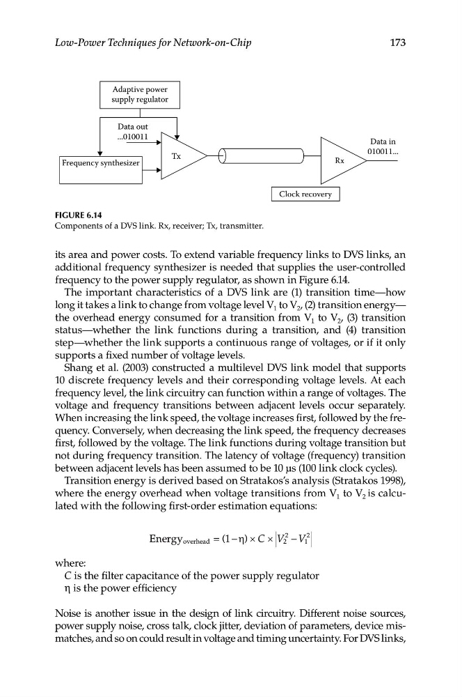
Figure 6.14
Components of a DVS link. Rx, receiver; Tx, transmitter.
its area and power costs. To extend variable frequency links to DVS links, an
additional frequency synthesizer is needed that supplies the user-controlled
frequency to the power supply regulator, as shown in Figure 6.14.
The important characteristics of a DVS link are (1) transition time—how
long it takes a link to change from voltage level V 1 to V 2 , (2) transition energy—
the overhead energy consumed for a transition from V 1 to V 2 , (3) transition
status—whether the link functions during a transition, and (4) transition
step—whether the link supports a continuous range of voltages, or if it only
supports a fixed number of voltage levels.
Shang et al. (2003) constructed a multilevel DVS link model that supports
10 discrete frequency levels and their corresponding voltage levels. At each
frequency level, the link circuitry can function within a range of voltages. The
voltage and frequency transitions between adjacent levels occur separately.
When increasing the link speed, the voltage increases first, followed by the frequency. Conversely, when decreasing the link speed, the frequency decreases
first, followed by the voltage. The link functions during voltage transition but
not during frequency transition. The latency of voltage (frequency) transition
between adjacent levels has been assumed to be 10 µs (100 link clock cycles).
Transition energy is derived based on Stratakos’s analysis (Stratakos 1998),
where the energy overhead when voltage transitions from V 1 to V 2 is calculated with the following first-order estimation equations:
Energy overhead = (1− η) × C × V 2
2
− V 1
2
where:
C is the filter capacitance of the power supply regulator
η is the power efficiency
Noise is another issue in the design of link circuitry. Different noise sources,
power supply noise, cross talk, clock jitter, deviation of parameters, device mismatches, and so on could result in voltage and timing uncertainty. For DVS links,