

171
Low-Power Techniques for Network-on-Chip
SOUT
MUXO
BUF
1
1
1
1
1
0
0
0
0
0
DE
DE
DE
DE
BUF
DE/2
STOP
EN
0
1
1
MUXP
D0
0
0
1
1
0
1
0
1
D1
D2
D3
Serializer
Deserializer
Q3
Q2
Q1
Q0
QS3
QS2
QS1
QP
0
DE
DE
DE
DE
DE
(pilot)
QS0
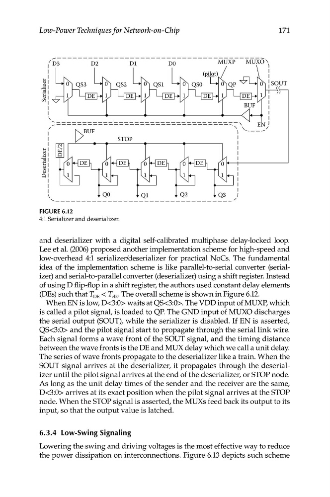
Figure 6.12
4:1 Serializer and deserializer.
and deserializer with a digital self-calibrated multiphase delay-locked loop.
Lee et al. (2006) proposed another implementation scheme for high-speed and
low-overhead 4:1 serializer/deserializer for practical NoCs. The fundamental
idea of the implementation scheme is like parallel-to-serial converter (serializer) and serial-to-parallel converter (deserializer) using a shift register. Instead
of using D flip-flop in a shift register, the authors used constant delay elements
(DEs) such that T DE < T clk . The overall scheme is shown in Figure 6.12.
When EN is low, D<3:0> waits at QS<3:0>. The VDD input of MUXP, which
is called a pilot signal, is loaded to QP. The GND input of MUXO discharges
the serial output (SOUT), while the serializer is disabled. If EN is asserted,
QS<3:0> and the pilot signal start to propagate through the serial link wire.
Each signal forms a wave front of the SOUT signal, and the timing distance
between the wave fronts is the DE and MUX delay which we call a unit delay.
The series of wave fronts propagate to the deserializer like a train. When the
SOUT signal arrives at the deserializer, it propagates through the deserializer until the pilot signal arrives at the end of the deserializer, or STOP node.
As long as the unit delay times of the sender and the receiver are the same,
D<3:0> arrives at its exact position when the pilot signal arrives at the STOP
node. When the STOP signal is asserted, the MUXs feed back its output to its
input, so that the output value is latched.
6.3.4 Low-Swing Signaling
Lowering the swing and driving voltages is the most effective way to reduce
the power dissipation on interconnections. Figure 6.13 depicts such scheme