

165
Low-Power Techniques for Network-on-Chip
timing is met, if some positive slack exists in the critical path, optimization
tools try to replace some of the lower V T cells with higher V T cells and/or with
cells having longer channel length. In case of noncritical path, optimization
tools also replace the same until they become the critical one.
6.2.5 Power gating
The principle of power gating is to selectively powering down certain blocks
in the chips while keeping other blocks powered up. The goal of power gating
is to minimize leakage current by temporarily switching some blocks to the
power-down mode that are not required to be in the active mode while minimizing the impact on performance. Power gating is more persistent than clock
gating that it affects interblock interface communication and adds significant
time delays to safely enter and exit the power-down mode. Power gating to
some portions of the design can be controlled by software as a part of device
drivers or initiated in hardware by timers or system-level power management
controllers. Architectural trade-offs in any power-gated design are as follows:
1. The amount of possible leakage power savings
2. The energy dissipated during entering and leaving such leakage
saving modes
3. Frequency of entering into the power gating and active modes
4. Performance penalty during entry and exit times
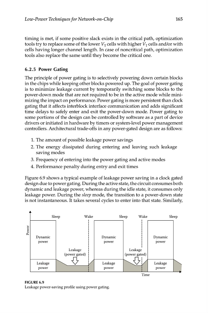
Figure 6.9 shows a typical example of leakage power saving in a clock gated
design due to power gating. During the active state, the circuit consumes both
dynamic and leakage power, whereas during the idle state, it consumes only
leakage power. During the sleep mode, the transition to a power-down state
is not instantaneous. It takes several cycles to enter into that state. Similarly,
Sleep
Dynamic
power
Leakage
power
Leakage
power
Leakage
power
Leakage
(power gated)
Dynamic
power
Dynamic
power
Power
Wake
Sleep
Wake
Sleep
Leakage
(power gated)
Time
Figure 6.9
Leakage power-saving profile using power gating.
Low-Power Techniques for Network-on-Chip
timing is met, if some positive slack exists in the critical path, optimization
tools try to replace some of the lower V T cells with higher V T cells and/or with
cells having longer channel length. In case of noncritical path, optimization
tools also replace the same until they become the critical one.
6.2.5 Power gating
The principle of power gating is to selectively powering down certain blocks
in the chips while keeping other blocks powered up. The goal of power gating
is to minimize leakage current by temporarily switching some blocks to the
power-down mode that are not required to be in the active mode while minimizing the impact on performance. Power gating is more persistent than clock
gating that it affects interblock interface communication and adds significant
time delays to safely enter and exit the power-down mode. Power gating to
some portions of the design can be controlled by software as a part of device
drivers or initiated in hardware by timers or system-level power management
controllers. Architectural trade-offs in any power-gated design are as follows:
1. The amount of possible leakage power savings
2. The energy dissipated during entering and leaving such leakage
saving modes
3. Frequency of entering into the power gating and active modes
4. Performance penalty during entry and exit times
Figure 6.9 shows a typical example of leakage power saving in a clock gated
design due to power gating. During the active state, the circuit consumes both
dynamic and leakage power, whereas during the idle state, it consumes only
leakage power. During the sleep mode, the transition to a power-down state
is not instantaneous. It takes several cycles to enter into that state. Similarly,
Sleep
Dynamic
power
Leakage
power
Leakage
power
Leakage
power
Leakage
(power gated)
Dynamic
power
Dynamic
power
Power
Wake
Sleep
Wake
Sleep
Leakage
(power gated)
Time
Figure 6.9
Leakage power-saving profile using power gating.