

164
Network-on-Chip
6.2.3.1.2 Placement of Level Shifter
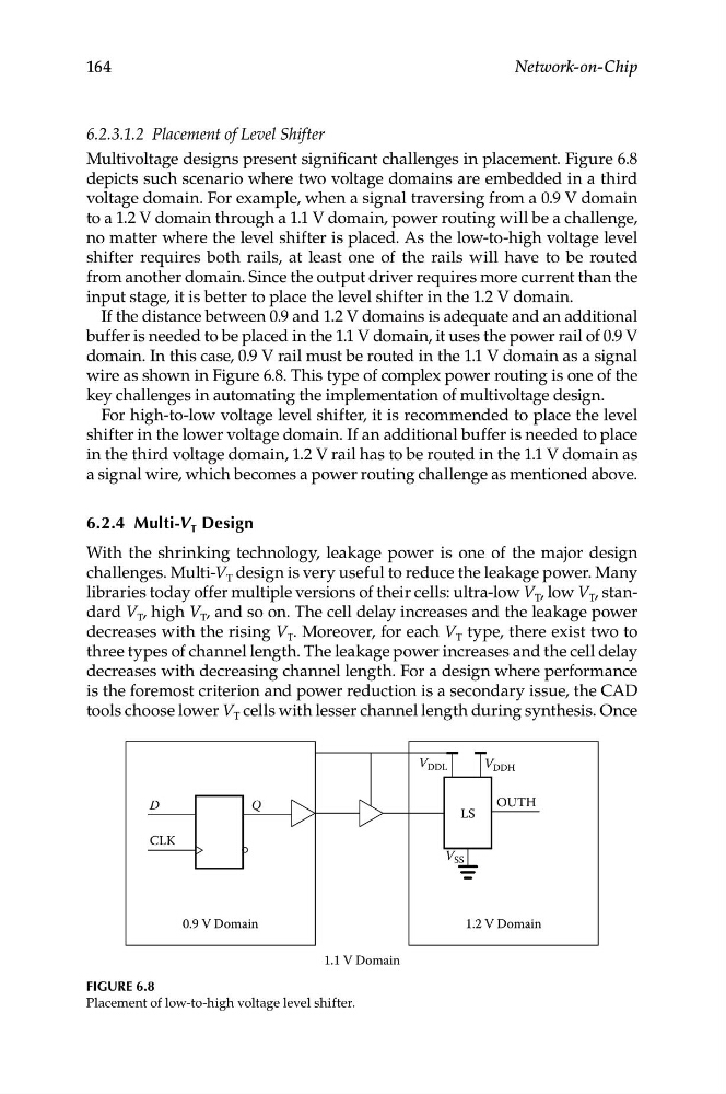
Multivoltage designs present significant challenges in placement. Figure 6.8
depicts such scenario where two voltage domains are embedded in a third
voltage domain. For example, when a signal traversing from a 0.9 V domain
to a 1.2 V domain through a 1.1 V domain, power routing will be a challenge,
no matter where the level shifter is placed. As the low-to-high voltage level
shifter requires both rails, at least one of the rails will have to be routed
from another domain. Since the output driver requires more current than the
input stage, it is better to place the level shifter in the 1.2 V domain.
If the distance between 0.9 and 1.2 V domains is adequate and an additional
buffer is needed to be placed in the 1.1 V domain, it uses the power rail of 0.9 V
domain. In this case, 0.9 V rail must be routed in the 1.1 V domain as a signal
wire as shown in Figure 6.8. This type of complex power routing is one of the
key challenges in automating the implementation of multivoltage design.
For high-to-low voltage level shifter, it is recommended to place the level
shifter in the lower voltage domain. If an additional buffer is needed to place
in the third voltage domain, 1.2 V rail has to be routed in the 1.1 V domain as
a signal wire, which becomes a power routing challenge as mentioned above.
6.2.4 Multi-V T Design
With the shrinking technology, leakage power is one of the major design
challenges. Multi-V T design is very useful to reduce the leakage power. Many
libraries today offer multiple versions of their cells: ultra-low V T , low V T , standard V T , high V T , and so on. The cell delay increases and the leakage power
decreases with the rising V T . Moreover, for each V T type, there exist two to
three types of channel length. The leakage power increases and the cell delay
decreases with decreasing channel length. For a design where performance
is the foremost criterion and power reduction is a secondary issue, the CAD
tools choose lower V T cells with lesser channel length during synthesis. Once
0.9 V Domain
D
Q
V DDL
V DDH
OUTH
LS
V SS
CLK
1.2 V Domain
1.1 V Domain
Figure 6.8
Placement of low-to-high voltage level shifter.