

161
Low-Power Techniques for Network-on-Chip
6.2.3.1 Challenges in Multivoltage Design
When a signal traverses from a low-voltage domain (V DDL ) to a high-voltage
domain (V DDH ) or vice versa, the circuit designers face several challenges as
follows:
6.2.3.1.1 Short-Circuit Current Flow
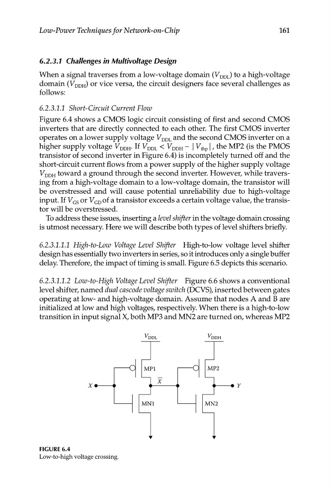
Figure 6.4 shows a CMOS logic circuit consisting of first and second CMOS
inverters that are directly connected to each other. The first CMOS inverter
operates on a lower supply voltage V DDL and the second CMOS inverter on a
higher supply voltage V DDH . If V DDL < V DDH – |V thp |, the MP2 (is the PMOS
transistor of second inverter in Figure 6.4) is incompletely turned off and the
short-circuit current flows from a power supply of the higher supply voltage
V DDH toward a ground through the second inverter. However, while traversing from a high-voltage domain to a low-voltage domain, the transistor will
be overstressed and will cause potential unreliability due to high-voltage
input. If V GS or V GD of a transistor exceeds a certain voltage value, the transistor will be overstressed.
To address these issues, inserting a level shifter in the voltage domain crossing
is utmost necessary. Here we will describe both types of level shifters briefly.
6.2.3.1.1.1 High-to-Low Voltage Level Shifter High-to-low voltage level shifter
design has essentially two inverters in series, so it introduces only a single buffer
delay. Therefore, the impact of timing is small. Figure 6.5 depicts this scenario.
6.2.3.1.1.2 Low-to-High Voltage Level Shifter Figure 6.6 shows a conventional
level shifter, named dual cascode voltage switch (DCVS), inserted between gates
operating at low- and high-voltage domain. Assume that nodes A and B are
initialized at low and high voltages, respectively. When there is a high-to-low
transition in input signal X, both MP3 and MN2 are turned on, whereas MP2
V DDL
V DDH
MP2
MN2
MN1
MP1
X
X
Y
Figure 6.4
Low-to-high voltage crossing.