

V DDL
V DDH
V DDH
V DDH
X
Y
V DDL
A
B
X
MP1
MP2
MP3
MP4
MN4
MN3
MN1
MN2
MP5
MN5
162
Network-on-Chip
V DDL
OUTL
V SS
INH
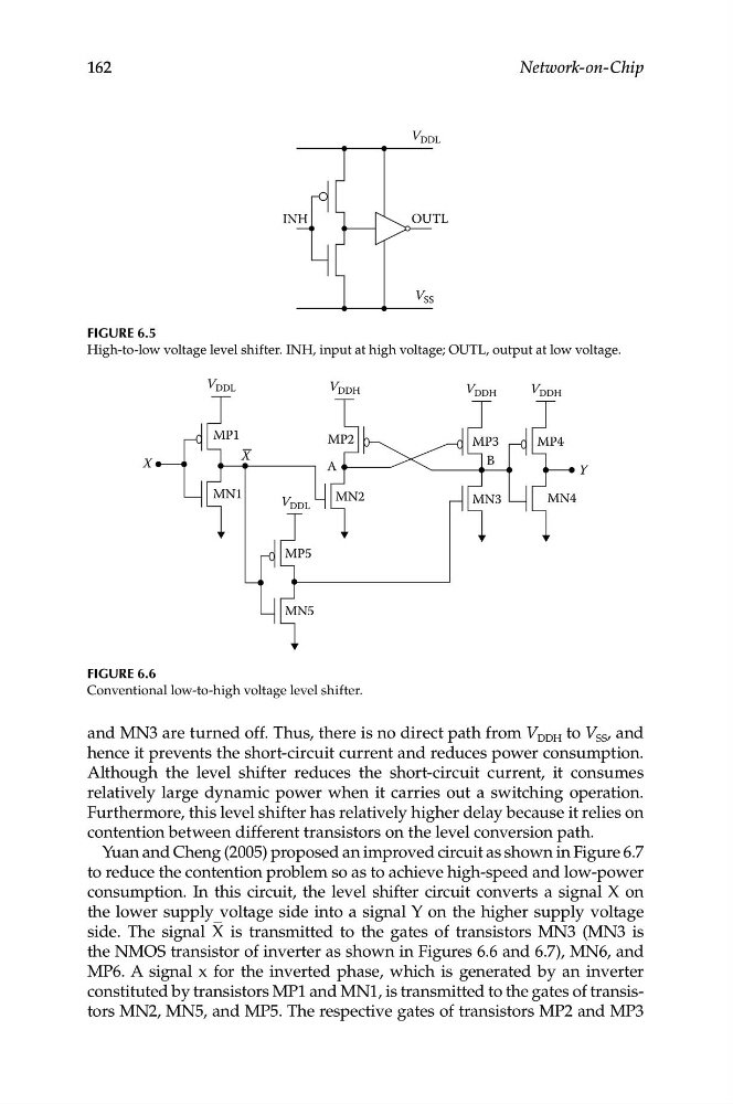
Figure 6.5
High-to-low voltage level shifter. INH, input at high voltage; OUTL, output at low voltage.
Figure 6.6
Conventional low-to-high voltage level shifter.
and MN3 are turned off. Thus, there is no direct path from V DDH to V SS , and
hence it prevents the short-circuit current and reduces power consumption.
Although the level shifter reduces the short-circuit current, it consumes
relatively large dynamic power when it carries out a switching operation.
Furthermore, this level shifter has relatively higher delay because it relies on
contention between different transistors on the level conversion path.
Yuan and Cheng (2005) proposed an improved circuit as shown in Figure 6.7
to reduce the contention problem so as to achieve high-speed and low-power
consumption. In this circuit, the level shifter circuit converts a signal X on
the lower supply voltage side into a signal Y on the higher supply voltage
side. The signal X is transmitted to the gates of transistors MN3 (MN3 is
the NMOS transistor of inverter as shown in Figures 6.6 and 6.7), MN6, and
MP6. A signal x for the inverted phase, which is generated by an inverter
constituted by transistors MP1 and MN1, is transmitted to the gates of transistors MN2, MN5, and MP5. The respective gates of transistors MP2 and MP3