

160
Network-on-Chip
2. Buffer insertion: If any driver drives a long net, it is good to break the
net by inserting buffer. This will improve both link delay and link
power consumption.
3. Cell sizing: Proper adjustment of cell size will reduce the delay and
also help to reduce dynamic power consumption.
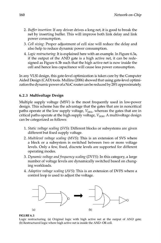
4. Logic restructuring: It is explained here with an example. In Figure 6.3a,
if the output of the AND gate is a high active net, it can be redesigned as Figure 6.3b such that the high active net is now inside the
cell and hence less capacitance will cause less power consumption.
In any VLSI design, this gate-level optimization is taken care by the Computer
Aided Design (CAD) tools. Mullins (2006) showed that using gate-level optimization the dynamic power of a NoC router can be reduced by 28% approximately.
6.2.3 Multivoltage Design
Multiple supply voltage (MSV) is the most frequently used in low-power
design. This scheme has the advantage that the gates that are in noncritical
paths operate at the low supply voltage, V DDL , whereas the gates that are in
critical paths operate at the high supply voltage, V DDH . A multivoltage design
can be categorized as follows:
1. Static voltage scaling (SVS): Different blocks or subsystems are given
different but fixed supply voltage.
2. Multilevel voltage scaling (MVS): This is an extension of SVS where
a block or a subsystem is switched between two or more voltage
levels. Only a few, fixed, discrete levels are supported for different
operating modes.
3. Dynamic voltage and frequency scaling (DVFS): In this category, a large
number of voltage levels are dynamically switched based on changing workloads.
4. Adaptive voltage scaling (AVS): This is an extension of DVFS where a
control loop is used to adjust the voltage.
(a)
(b)
Figure 6.3
Logic restructuring. (a) Original logic with high active net at the output of AND gate;
(b) Restructured logic where high active net is inside the AND–OR cell.