

159
Low-Power Techniques for Network-on-Chip
edge-triggered D flip-flop is used for this purpose. The input data to FIFO
(data_in) and write enable (wr_en) signals are synchronous with the rising
edge of wr_clk. When the network is idle, the data_in signal becomes invalid
and the wr_en signal is at logic 0. Hence, the gated write clock (gclk) becomes
active low. This gclk signal is again gated with the individual write enable
signals (selected by the decoder) of the registers to perform register-level
clock gating inside the FIFO. It is obvious that the clock gating in the write
registers does not introduce any additional cycle latency in the FIFO.
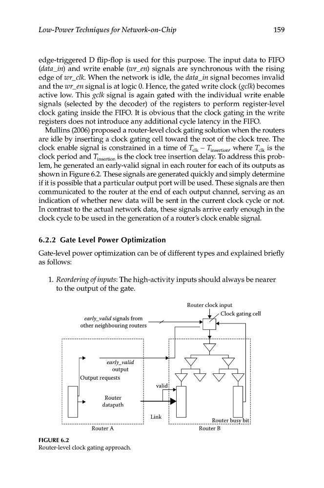
Mullins (2006) proposed a router-level clock gating solution when the routers
are idle by inserting a clock gating cell toward the root of the clock tree. The
clock enable signal is constrained in a time of T clk – T insertion , where T clk is the
clock period and T insertion is the clock tree insertion delay. To address this problem, he generated an early-valid signal in each router for each of its outputs as
shown in Figure 6.2. These signals are generated quickly and simply determine
if it is possible that a particular output port will be used. These signals are then
communicated to the router at the end of each output channel, serving as an
indication of whether new data will be sent in the current clock cycle or not.
In contrast to the actual network data, these signals arrive early enough in the
clock cycle to be used in the generation of a router’s clock enable signal.
6.2.2 gate Level Power Optimization
Gate-level power optimization can be of different types and explained briefly
as follows:
1. Reordering of inputs: The high-activity inputs should always be nearer
to the output of the gate.
early_valid signals from
other neighbouring routers
Router clock input
Clock gating cell
Router busy bit
Router B
Link
valid
early_valid
output
Output requests
Router
datapath
Router A
Figure 6.2
Router-level clock gating approach.