

158
Network-on-Chip
6.2 Standard Low-Power Methods for NoC Routers
There are a number of power reduction techniques that have been widely used
in Very Large Scale Integration (VLSI) design and also adopted in NoC router.
This section gives an overview of the following methods: (1) clock gating, (2)
gate-level power optimization, (3) multi-V DD , (4) multi-V T , and (5) power gating.
6.2.1 Clock gating
The internal node switching power is dominated by the transition of clock
in any sequential design. With every clock transition, the capacitances internal to the cell are either charging or discharging, and hence consume very
high internal power. It can be observed from Figure 4.14 that the change in
the total router energy consumption is not significant with variation in the
offered load. The routers consume a significant amount of energy even at
very low traffic, though switching of input data is low. This appears as the
internal power consumption due to free-running clock dominates over the
switching and leakage power. Therefore, to reduce the internal power, it is
essential to stop the free-running clock, when the network is idle.
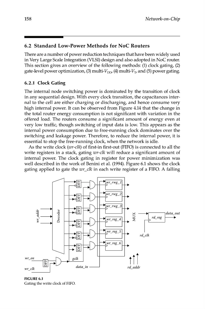
As the write clock (wr-clk) of first-in first-out (FIFO) is connected to all the
write registers in a stack, gating wr-clk will reduce a significant amount of
internal power. The clock gating in register for power minimization was
well described in the work of Benini et al. (1994). Figure 6.1 shows the clock
gating applied to gate the wr_clk in each write register of a FIFO. A falling
Decoder
DFF
DFF
DFF
DFF
gclk
data_in
wr_en
wr_addr
rd_addr
wr_clk
rd_clk
rd_reg
data_out
wr_rwg _3
wr_reg _4
MUX
wr_reg _5
wr_reg _6
wr_rwg _1
wr_rwg _2
DFF
DFF
DFF
Figure 6.1
Gating the write clock of FIFO.
Network-on-Chip
6.2 Standard Low-Power Methods for NoC Routers
There are a number of power reduction techniques that have been widely used
in Very Large Scale Integration (VLSI) design and also adopted in NoC router.
This section gives an overview of the following methods: (1) clock gating, (2)
gate-level power optimization, (3) multi-V DD , (4) multi-V T , and (5) power gating.
6.2.1 Clock gating
The internal node switching power is dominated by the transition of clock
in any sequential design. With every clock transition, the capacitances internal to the cell are either charging or discharging, and hence consume very
high internal power. It can be observed from Figure 4.14 that the change in
the total router energy consumption is not significant with variation in the
offered load. The routers consume a significant amount of energy even at
very low traffic, though switching of input data is low. This appears as the
internal power consumption due to free-running clock dominates over the
switching and leakage power. Therefore, to reduce the internal power, it is
essential to stop the free-running clock, when the network is idle.
As the write clock (wr-clk) of first-in first-out (FIFO) is connected to all the
write registers in a stack, gating wr-clk will reduce a significant amount of
internal power. The clock gating in register for power minimization was
well described in the work of Benini et al. (1994). Figure 6.1 shows the clock
gating applied to gate the wr_clk in each write register of a FIFO. A falling
Decoder
DFF
DFF
DFF
DFF
gclk
data_in
wr_en
wr_addr
rd_addr
wr_clk
rd_clk
rd_reg
data_out
wr_rwg _3
wr_reg _4
MUX
wr_reg _5
wr_reg _6
wr_rwg _1
wr_rwg _2
DFF
DFF
DFF
Figure 6.1
Gating the write clock of FIFO.