

94
Network-on-Chip
Source
Source
d = 0
d = 1
d = 0
d = 2 d = 3
d = 4
d = 5
d = 6
d = 2
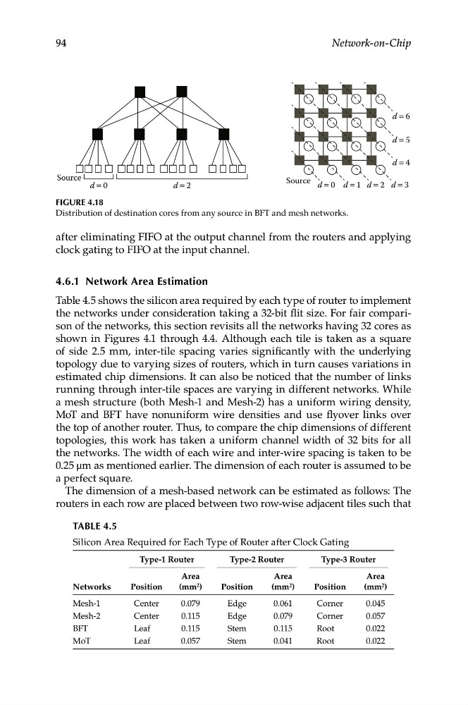
Figure 4.18
Distribution of destination cores from any source in BFT and mesh networks.
after eliminating FIFO at the output channel from the routers and applying
clock gating to FIFO at the input channel.
4.6.1 Network Area estimation
Table 4.5 shows the silicon area required by each type of router to implement
the networks under consideration taking a 32-bit flit size. For fair comparison of the networks, this section revisits all the networks having 32 cores as
shown in Figures 4.1 through 4.4. Although each tile is taken as a square
of side 2.5 mm, inter-tile spacing varies significantly with the underlying
topology due to varying sizes of routers, which in turn causes variations in
estimated chip dimensions. It can also be noticed that the number of links
running through inter-tile spaces are varying in different networks. While
a mesh structure (both Mesh-1 and Mesh-2) has a uniform wiring density,
MoT and BFT have nonuniform wire densities and use flyover links over
the top of another router. Thus, to compare the chip dimensions of different
topologies, this work has taken a uniform channel width of 32 bits for all
the networks. The width of each wire and inter-wire spacing is taken to be
0.25 µm as mentioned earlier. The dimension of each router is assumed to be
a perfect square.
The dimension of a mesh-based network can be estimated as follows: The
routers in each row are placed between two row-wise adjacent tiles such that
TABLe 4.5
Silicon Area Required for Each Type of Router after Clock Gating
Type-1 Router
Type-2 Router
Type-3 Router
Area
Area
Area
Networks
Position
(mm 2 )
Position
(mm 2 )
Position
(mm 2 )
Mesh-1
Center
0.079
Edge
0.061
Corner
0.045
Mesh-2
Center
0.115
Edge
0.079
Corner
0.057
BFT
Leaf
0.115
Stem
0.115
Root
0.022
MoT
Leaf
0.057
Stem
0.041
Root
0.022
Network-on-Chip
Source
Source
d = 0
d = 1
d = 0
d = 2 d = 3
d = 4
d = 5
d = 6
d = 2
Figure 4.18
Distribution of destination cores from any source in BFT and mesh networks.
after eliminating FIFO at the output channel from the routers and applying
clock gating to FIFO at the input channel.
4.6.1 Network Area estimation
Table 4.5 shows the silicon area required by each type of router to implement
the networks under consideration taking a 32-bit flit size. For fair comparison of the networks, this section revisits all the networks having 32 cores as
shown in Figures 4.1 through 4.4. Although each tile is taken as a square
of side 2.5 mm, inter-tile spacing varies significantly with the underlying
topology due to varying sizes of routers, which in turn causes variations in
estimated chip dimensions. It can also be noticed that the number of links
running through inter-tile spaces are varying in different networks. While
a mesh structure (both Mesh-1 and Mesh-2) has a uniform wiring density,
MoT and BFT have nonuniform wire densities and use flyover links over
the top of another router. Thus, to compare the chip dimensions of different
topologies, this work has taken a uniform channel width of 32 bits for all
the networks. The width of each wire and inter-wire spacing is taken to be
0.25 µm as mentioned earlier. The dimension of each router is assumed to be
a perfect square.
The dimension of a mesh-based network can be estimated as follows: The
routers in each row are placed between two row-wise adjacent tiles such that
TABLe 4.5
Silicon Area Required for Each Type of Router after Clock Gating
Type-1 Router
Type-2 Router
Type-3 Router
Area
Area
Area
Networks
Position
(mm 2 )
Position
(mm 2 )
Position
(mm 2 )
Mesh-1
Center
0.079
Edge
0.061
Corner
0.045
Mesh-2
Center
0.115
Edge
0.079
Corner
0.057
BFT
Leaf
0.115
Stem
0.115
Root
0.022
MoT
Leaf
0.057
Stem
0.041
Root
0.022