

228
N. Wade et al.
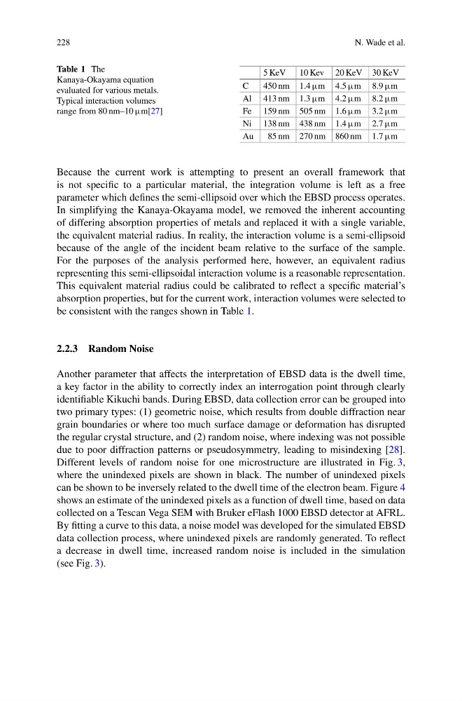
Table 1 The
Kanaya-Okayama equation
evaluated for various metals.
Typical interaction volumes
range from 80 nm–10 μm[27]
5 KeV
10 Kev 20 KeV 30 KeV
C
450 nm 1.4 μm 4.5 μm 8.9 μm
Al 413 nm 1.3 μm 4.2 μm 8.2 μm
Fe 159 nm 505 nm 1.6 μm 3.2 μm
Ni 138 nm 438 nm 1.4 μm 2.7 μm
Au
85 nm 270 nm 860 nm 1.7 μm
Because the current work is attempting to present an overall framework that
is not specific to a particular material, the integration volume is left as a free
parameter which defines the semi-ellipsoid over which the EBSD process operates.
In simplifying the Kanaya-Okayama model, we removed the inherent accounting
of differing absorption properties of metals and replaced it with a single variable,
the equivalent material radius. In reality, the interaction volume is a semi-ellipsoid
because of the angle of the incident beam relative to the surface of the sample.
For the purposes of the analysis performed here, however, an equivalent radius
representing this semi-ellipsoidal interaction volume is a reasonable representation.
This equivalent material radius could be calibrated to reflect a specific material’s
absorption properties, but for the current work, interaction volumes were selected to
be consistent with the ranges shown in Table 1.
2.2.3 Random Noise
Another parameter that affects the interpretation of EBSD data is the dwell time,
a key factor in the ability to correctly index an interrogation point through clearly
identifiable Kikuchi bands. During EBSD, data collection error can be grouped into
two primary types: (1) geometric noise, which results from double diffraction near
grain boundaries or where too much surface damage or deformation has disrupted
the regular crystal structure, and (2) random noise, where indexing was not possible
due to poor diffraction patterns or pseudosymmetry, leading to misindexing [28].
Different levels of random noise for one microstructure are illustrated in Fig. 3,
where the unindexed pixels are shown in black. The number of unindexed pixels
can be shown to be inversely related to the dwell time of the electron beam. Figure 4
shows an estimate of the unindexed pixels as a function of dwell time, based on data
collected on a Tescan Vega SEM with Bruker eFlash 1000 EBSD detector at AFRL.
By fitting a curve to this data, a noise model was developed for the simulated EBSD
data collection process, where unindexed pixels are randomly generated. To reflect
a decrease in dwell time, increased random noise is included in the simulation
(see Fig. 3).
N. Wade et al.
Table 1 The
Kanaya-Okayama equation
evaluated for various metals.
Typical interaction volumes
range from 80 nm–10 μm[27]
5 KeV
10 Kev 20 KeV 30 KeV
C
450 nm 1.4 μm 4.5 μm 8.9 μm
Al 413 nm 1.3 μm 4.2 μm 8.2 μm
Fe 159 nm 505 nm 1.6 μm 3.2 μm
Ni 138 nm 438 nm 1.4 μm 2.7 μm
Au
85 nm 270 nm 860 nm 1.7 μm
Because the current work is attempting to present an overall framework that
is not specific to a particular material, the integration volume is left as a free
parameter which defines the semi-ellipsoid over which the EBSD process operates.
In simplifying the Kanaya-Okayama model, we removed the inherent accounting
of differing absorption properties of metals and replaced it with a single variable,
the equivalent material radius. In reality, the interaction volume is a semi-ellipsoid
because of the angle of the incident beam relative to the surface of the sample.
For the purposes of the analysis performed here, however, an equivalent radius
representing this semi-ellipsoidal interaction volume is a reasonable representation.
This equivalent material radius could be calibrated to reflect a specific material’s
absorption properties, but for the current work, interaction volumes were selected to
be consistent with the ranges shown in Table 1.
2.2.3 Random Noise
Another parameter that affects the interpretation of EBSD data is the dwell time,
a key factor in the ability to correctly index an interrogation point through clearly
identifiable Kikuchi bands. During EBSD, data collection error can be grouped into
two primary types: (1) geometric noise, which results from double diffraction near
grain boundaries or where too much surface damage or deformation has disrupted
the regular crystal structure, and (2) random noise, where indexing was not possible
due to poor diffraction patterns or pseudosymmetry, leading to misindexing [28].
Different levels of random noise for one microstructure are illustrated in Fig. 3,
where the unindexed pixels are shown in black. The number of unindexed pixels
can be shown to be inversely related to the dwell time of the electron beam. Figure 4
shows an estimate of the unindexed pixels as a function of dwell time, based on data
collected on a Tescan Vega SEM with Bruker eFlash 1000 EBSD detector at AFRL.
By fitting a curve to this data, a noise model was developed for the simulated EBSD
data collection process, where unindexed pixels are randomly generated. To reflect
a decrease in dwell time, increased random noise is included in the simulation
(see Fig. 3).