

75
Review of Basic Device Physics
the junction grading coefficient, resulting in the following generalized equation for C j as
C
C
V
j
j
d
bi
mj
=
− (
)
0
1
φ
(2.139)
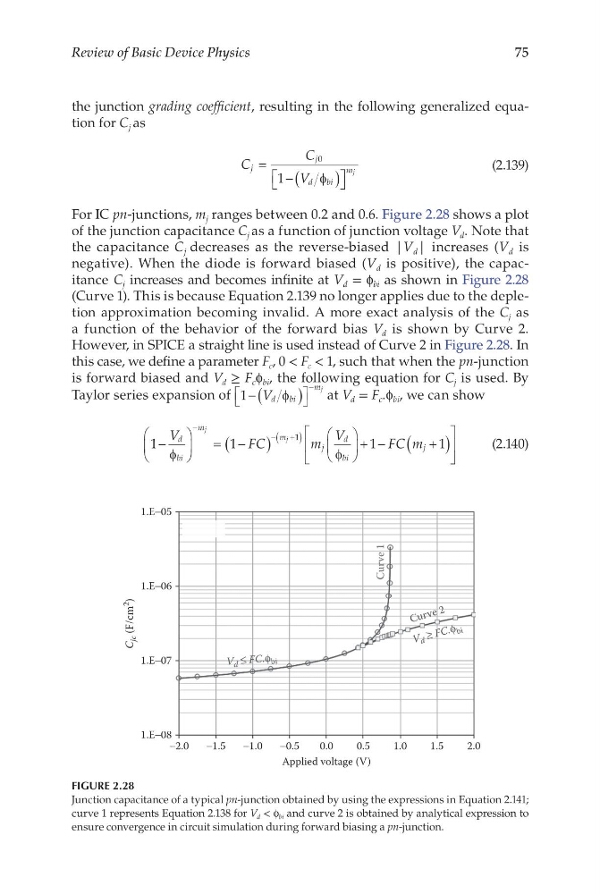
For IC pn-junctions, m j ranges between 0.2 and 0.6. Figure 2.28 shows a plot
of the junction capacitance C j as a function of junction voltage V d . Note that
the capacitance C j decreases as the reverse-biased |V d | increases (V d is
negative). When the diode is forward biased (V d is positive), the capacitance C j increases and becomes infinite at V d = f bi as shown in Figure 2.28
(Curve 1). This is because Equation 2.139 no longer applies due to the depletion approximation becoming invalid. A more exact analysis of the C j as
a function of the behavior of the forward bias V d is shown by Curve 2.
However, in SPICE a straight line is used instead of Curve 2 in Figure 2.28. In
this case, we define a parameter F c , 0 < F c < 1, such that when the pn-junction
is forward biased and V d ≥ F c f bi , the following equation for C j is used. By
Taylor series expansion of 1− (
)
−
V d bi
mj
φ
at V d = F c .f bi , we can show
1
1
1
1
1
−
= −
(
)
+ −
+
(
)
−
−
+
(
)
V
FC
m
V
FC m
d
bi
m
m
j
d
bi
j
j
j
φ
φ
(2.140)
−2.0
−1.5
−1.0
−0.5
0.0
Applied voltage (V)
1.E−08
1.E−07
V d ≤ FC.ϕbi
Vd ≥ F C .ϕbi
C
jc (F/cm
2
)
1.E−06
Curve 1
C u rv e 2
1.E−05
0.5
1.0
1.5
2.0
FIGURE 2.28
Junction capacitance of a typical pn-junction obtained by using the expressions in Equation 2.141;
curve 1 represents Equation 2.138 for V d < f bi and curve 2 is obtained by analytical expression to
ensure convergence in circuit simulation during forward biasing a pn-junction.
Review of Basic Device Physics
the junction grading coefficient, resulting in the following generalized equation for C j as
C
C
V
j
j
d
bi
mj
=
− (
)
0
1
φ
(2.139)
For IC pn-junctions, m j ranges between 0.2 and 0.6. Figure 2.28 shows a plot
of the junction capacitance C j as a function of junction voltage V d . Note that
the capacitance C j decreases as the reverse-biased |V d | increases (V d is
negative). When the diode is forward biased (V d is positive), the capacitance C j increases and becomes infinite at V d = f bi as shown in Figure 2.28
(Curve 1). This is because Equation 2.139 no longer applies due to the depletion approximation becoming invalid. A more exact analysis of the C j as
a function of the behavior of the forward bias V d is shown by Curve 2.
However, in SPICE a straight line is used instead of Curve 2 in Figure 2.28. In
this case, we define a parameter F c , 0 < F c < 1, such that when the pn-junction
is forward biased and V d ≥ F c f bi , the following equation for C j is used. By
Taylor series expansion of 1− (
)
−
V d bi
mj
φ
at V d = F c .f bi , we can show
1
1
1
1
1
−
= −
(
)
+ −
+
(
)
−
−
+
(
)
V
FC
m
V
FC m
d
bi
m
m
j
d
bi
j
j
j
φ
φ
(2.140)
−2.0
−1.5
−1.0
−0.5
0.0
Applied voltage (V)
1.E−08
1.E−07
V d ≤ FC.ϕbi
Vd ≥ F C .ϕbi
C
jc (F/cm
2
)
1.E−06
Curve 1
C u rv e 2
1.E−05
0.5
1.0
1.5
2.0
FIGURE 2.28
Junction capacitance of a typical pn-junction obtained by using the expressions in Equation 2.141;
curve 1 represents Equation 2.138 for V d < f bi and curve 2 is obtained by analytical expression to
ensure convergence in circuit simulation during forward biasing a pn-junction.