

76
Compact Models for Integrated Circuit Design
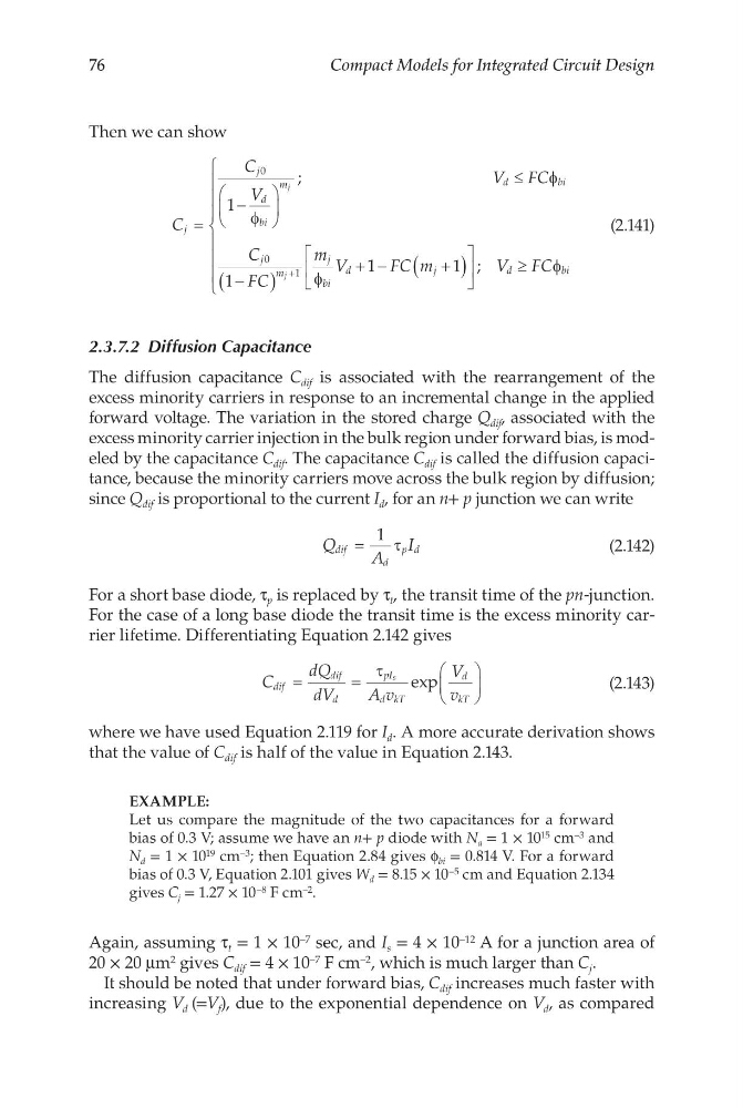
Then we can show
C
C
V
V FC
C
FC
m V
j
j
d
bi
m
d
b i
j
m
j
bi
d
j
j
=
−
≤
−
(
)
+
+
0
0
1
1
1
φ
φ
φ
;
1 1
1
−
+
(
)
≥
FC m
V FC
j
d
bi
;
φ
(2.141)
2.3.7.2 Diffusion Capacitance
The diffusion capacitance C dif is associated with the rearrangement of the
excess minority carriers in response to an incremental change in the applied
forward voltage. The variation in the stored charge Q dif , associated with the
excess minority carrier injection in the bulk region under forward bias, is modeled by the capacitance C dif . The capacitance C dif is called the diffusion capacitance, because the minority carriers move across the bulk region by diffusion;
since Q dif is proportional to the current I d , for an n+ p junction we can write
Q
A
I
d
p d
dif =
1 τ
(2.142)
For a short base diode, τ p is replaced by τ t , the transit time of the pn-junction.
For the case of a long base diode the transit time is the excess minority carrier lifetime. Differentiating Equation 2.142 gives
C
dQ
dV
A v
V
v
d
pI
d kT
d
kT
s
dif
dif
=
=
τ
exp
(2.143)
where we have used Equation 2.119 for I d . A more accurate derivation shows
that the value of C dif is half of the value in Equation 2.143.
EXAMPLE:
Let us compare the magnitude of the two capacitances for a forward
bias of 0.3 V; assume we have an n+ p diode with N a = 1 × 10 15 cm –3 and
N d = 1 × 10 19 cm –3 ; then Equation 2.84 gives f bi = 0.814 V. For a forward
bias of 0.3 V, Equation 2.101 gives W d = 8.15 × 10 –5 cm and Equation 2.134
gives C j = 1.27 × 10 –8 F cm –2 .
Again, assuming τ t = 1 × 10 –7 sec, and I s = 4 × 10 –12 A for a junction area of
20 × 20 μm 2 gives C dif = 4 × 10 –7 F cm –2 , which is much larger than C j .
It should be noted that under forward bias, C dif increases much faster with
increasing V d (=V f ), due to the exponential dependence on V d , as compared
Compact Models for Integrated Circuit Design
Then we can show
C
C
V
V FC
C
FC
m V
j
j
d
bi
m
d
b i
j
m
j
bi
d
j
j
=
−
≤
−
(
)
+
+
0
0
1
1
1
φ
φ
φ
;
1 1
1
−
+
(
)
≥
FC m
V FC
j
d
bi
;
φ
(2.141)
2.3.7.2 Diffusion Capacitance
The diffusion capacitance C dif is associated with the rearrangement of the
excess minority carriers in response to an incremental change in the applied
forward voltage. The variation in the stored charge Q dif , associated with the
excess minority carrier injection in the bulk region under forward bias, is modeled by the capacitance C dif . The capacitance C dif is called the diffusion capacitance, because the minority carriers move across the bulk region by diffusion;
since Q dif is proportional to the current I d , for an n+ p junction we can write
Q
A
I
d
p d
dif =
1 τ
(2.142)
For a short base diode, τ p is replaced by τ t , the transit time of the pn-junction.
For the case of a long base diode the transit time is the excess minority carrier lifetime. Differentiating Equation 2.142 gives
C
dQ
dV
A v
V
v
d
pI
d kT
d
kT
s
dif
dif
=
=
τ
exp
(2.143)
where we have used Equation 2.119 for I d . A more accurate derivation shows
that the value of C dif is half of the value in Equation 2.143.
EXAMPLE:
Let us compare the magnitude of the two capacitances for a forward
bias of 0.3 V; assume we have an n+ p diode with N a = 1 × 10 15 cm –3 and
N d = 1 × 10 19 cm –3 ; then Equation 2.84 gives f bi = 0.814 V. For a forward
bias of 0.3 V, Equation 2.101 gives W d = 8.15 × 10 –5 cm and Equation 2.134
gives C j = 1.27 × 10 –8 F cm –2 .
Again, assuming τ t = 1 × 10 –7 sec, and I s = 4 × 10 –12 A for a junction area of
20 × 20 μm 2 gives C dif = 4 × 10 –7 F cm –2 , which is much larger than C j .
It should be noted that under forward bias, C dif increases much faster with
increasing V d (=V f ), due to the exponential dependence on V d , as compared