

59
Review of Basic Device Physics
W
K
q
N
N
V
d
si
a
d
bi
d
=
+
−
(
)
2
1
1
0
ε
φ
.
(2.101)
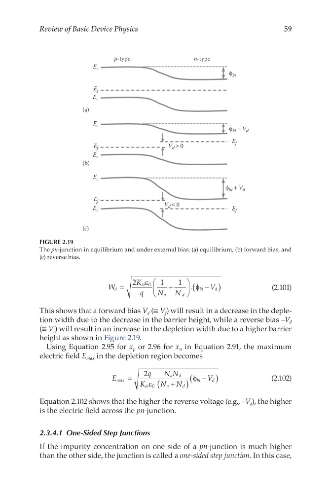
This shows that a forward bias V d (≡ V f ) will result in a decrease in the depletion width due to the decrease in the barrier height, while a reverse bias –V d
(≡ V r ) will result in an increase in the depletion width due to a higher barrier
height as shown in Figure 2.19.
Using Equation 2.95 for x p or 2.96 for x n in Equation 2.91, the maximum
electric field E max in the depletion region becomes
E
q
K
N N
N N
V
max
si
a d
a
d
bi
d
=
+
(
)
−
(
)
2
0
ε
φ
(2.102)
Equation 2.102 shows that the higher the reverse voltage (e.g., –V d ), the higher
is the electric field across the pn-junction.
2.3.4.1 One-Sided Step Junctions
If the impurity concentration on one side of a pn-junction is much higher
than the other side, the junction is called a one-sided step junction. In this case,
E c
p-type
n-type
E f
E v
ϕ bi
E c
E f
E f
ϕ bi + V d
E v
V d < 0
E c
E f
E v
E f
ϕ bi − V d
V d > 0
(a)
(b)
(c)
FIGURE 2.19
The pn-junction in equilibrium and under external bias: (a) equilibrium, (b) forward bias, and
(c) reverse bias.
Review of Basic Device Physics
W
K
q
N
N
V
d
si
a
d
bi
d
=
+
−
(
)
2
1
1
0
ε
φ
.
(2.101)
This shows that a forward bias V d (≡ V f ) will result in a decrease in the depletion width due to the decrease in the barrier height, while a reverse bias –V d
(≡ V r ) will result in an increase in the depletion width due to a higher barrier
height as shown in Figure 2.19.
Using Equation 2.95 for x p or 2.96 for x n in Equation 2.91, the maximum
electric field E max in the depletion region becomes
E
q
K
N N
N N
V
max
si
a d
a
d
bi
d
=
+
(
)
−
(
)
2
0
ε
φ
(2.102)
Equation 2.102 shows that the higher the reverse voltage (e.g., –V d ), the higher
is the electric field across the pn-junction.
2.3.4.1 One-Sided Step Junctions
If the impurity concentration on one side of a pn-junction is much higher
than the other side, the junction is called a one-sided step junction. In this case,
E c
p-type
n-type
E f
E v
ϕ bi
E c
E f
E f
ϕ bi + V d
E v
V d < 0
E c
E f
E v
E f
ϕ bi − V d
V d > 0
(a)
(b)
(c)
FIGURE 2.19
The pn-junction in equilibrium and under external bias: (a) equilibrium, (b) forward bias, and
(c) reverse bias.