

60
Compact Models for Integrated Circuit Design
the depletion region extends almost totally into the lighter doped side. For
example, in the case of an n+ p junction (N d >> N a and x n << x p ), the depletion
width W d is almost entirely in the p-side. Thus, from Equation 2.101, we can
show that the general expression for W d for a one-sided step junction is
W
K
qN
V
d
si
b
bi
d
=
±
(
)
2
0
ε φ
.
(2.103)
where:
N b = N a for n+ p junction
N b = N d for p+ n junction
A more accurate result for the depletion width can be obtained by considering
the majority carrier distribution tails or spillover (electrons in the n-side and
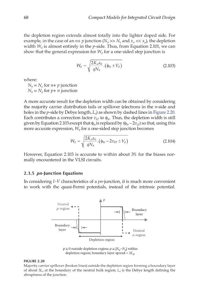
holes in the p-side by Debye length, L d ) as shown by dashed lines in Figure 2.20.
Each contributes a correction factor v kT to f bi . Thus, the depletion width is still
given by Equation 2.103 except that f bi is replaced by (f bi – 2v kT ) so that, using this
more accurate expression, W d for a one-sided step junction becomes
W
K
qN
v
V
d
si
b
bi
kT
d
=
−
±
(
)
2
2
0
ε φ
.
(2.104)
However, Equation 2.103 is accurate to within about 3% for the biases normally encountered in the VLSI circuits.
2.3.5 pn-Junction Equations
In considering I–V characteristics of a pn-junction, it is much more convenient
to work with the quasi-Fermi potentials, instead of the intrinsic potential.
Neutral
p-region
Boundary
layer
Boundary
layer
Neutral
n-region
Depletion region
ρ ≅ 0 outside depletion region; ρ ≅ |N a −N d | within
depletion region; boundary layer spread ≈ 3L d .
ρ
FIGURE 2.20
Majority carrier spillover (broken lines) outside the depletion region forming a boundary layer
of about 3L d at the boundary of the neutral bulk region; L d is the Debye length defining the
abruptness of the junction.
Compact Models for Integrated Circuit Design
the depletion region extends almost totally into the lighter doped side. For
example, in the case of an n+ p junction (N d >> N a and x n << x p ), the depletion
width W d is almost entirely in the p-side. Thus, from Equation 2.101, we can
show that the general expression for W d for a one-sided step junction is
W
K
qN
V
d
si
b
bi
d
=
±
(
)
2
0
ε φ
.
(2.103)
where:
N b = N a for n+ p junction
N b = N d for p+ n junction
A more accurate result for the depletion width can be obtained by considering
the majority carrier distribution tails or spillover (electrons in the n-side and
holes in the p-side by Debye length, L d ) as shown by dashed lines in Figure 2.20.
Each contributes a correction factor v kT to f bi . Thus, the depletion width is still
given by Equation 2.103 except that f bi is replaced by (f bi – 2v kT ) so that, using this
more accurate expression, W d for a one-sided step junction becomes
W
K
qN
v
V
d
si
b
bi
kT
d
=
−
±
(
)
2
2
0
ε φ
.
(2.104)
However, Equation 2.103 is accurate to within about 3% for the biases normally encountered in the VLSI circuits.
2.3.5 pn-Junction Equations
In considering I–V characteristics of a pn-junction, it is much more convenient
to work with the quasi-Fermi potentials, instead of the intrinsic potential.
Neutral
p-region
Boundary
layer
Boundary
layer
Neutral
n-region
Depletion region
ρ ≅ 0 outside depletion region; ρ ≅ |N a −N d | within
depletion region; boundary layer spread ≈ 3L d .
ρ
FIGURE 2.20
Majority carrier spillover (broken lines) outside the depletion region forming a boundary layer
of about 3L d at the boundary of the neutral bulk region; L d is the Debye length defining the
abruptness of the junction.