

58
Compact Models for Integrated Circuit Design
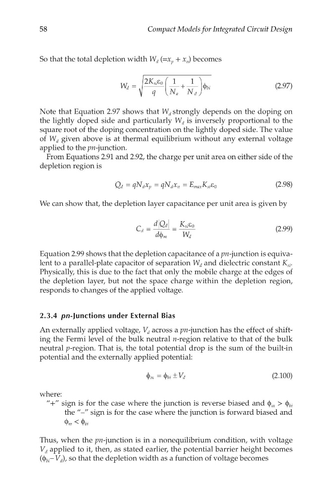
So that the total depletion width W d (=x p + x n ) becomes
W
K
q
N
N
d
si
a
d
bi
=
+
2
1
1
0
ε
φ
(2.97)
Note that Equation 2.97 shows that W d strongly depends on the doping on
the lightly doped side and particularly W d is inversely proportional to the
square root of the doping concentration on the lightly doped side. The value
of W d given above is at thermal equilibrium without any external voltage
applied to the pn-junction.
From Equations 2.91 and 2.92, the charge per unit area on either side of the
depletion region is
Q
qN x
qN x
E K
d
d p
d n
m ax si
=
=
=
ε 0
(2.98)
We can show that, the depletion layer capacitance per unit area is given by
C
d Q
d
K
W
d
d
m
si
d
=
=
φ
ε 0
(2.99)
Equation 2.99 shows that the depletion capacitance of a pn-junction is equivalent to a parallel-plate capacitor of separation W d and dielectric constant K si .
Physically, this is due to the fact that only the mobile charge at the edges of
the depletion layer, but not the space charge within the depletion region,
responds to changes of the applied voltage.
2.3.4 pn-Junctions under External Bias
An externally applied voltage, V d across a pn-junction has the effect of shifting the Fermi level of the bulk neutral n-region relative to that of the bulk
neutral p-region. That is, the total potential drop is the sum of the built-in
potential and the externally applied potential:
φ
φ
m
b i
d
V
=
±
(2.100)
where:
“+” sign is for the case where the junction is reverse biased and f m > f bi
the “–” sign is for the case where the junction is forward biased and
f m < f bi
Thus, when the pn-junction is in a nonequilibrium condition, with voltage
V d applied to it, then, as stated earlier, the potential barrier height becomes
(f bi – V d ), so that the depletion width as a function of voltage becomes
Compact Models for Integrated Circuit Design
So that the total depletion width W d (=x p + x n ) becomes
W
K
q
N
N
d
si
a
d
bi
=
+
2
1
1
0
ε
φ
(2.97)
Note that Equation 2.97 shows that W d strongly depends on the doping on
the lightly doped side and particularly W d is inversely proportional to the
square root of the doping concentration on the lightly doped side. The value
of W d given above is at thermal equilibrium without any external voltage
applied to the pn-junction.
From Equations 2.91 and 2.92, the charge per unit area on either side of the
depletion region is
Q
qN x
qN x
E K
d
d p
d n
m ax si
=
=
=
ε 0
(2.98)
We can show that, the depletion layer capacitance per unit area is given by
C
d Q
d
K
W
d
d
m
si
d
=
=
φ
ε 0
(2.99)
Equation 2.99 shows that the depletion capacitance of a pn-junction is equivalent to a parallel-plate capacitor of separation W d and dielectric constant K si .
Physically, this is due to the fact that only the mobile charge at the edges of
the depletion layer, but not the space charge within the depletion region,
responds to changes of the applied voltage.
2.3.4 pn-Junctions under External Bias
An externally applied voltage, V d across a pn-junction has the effect of shifting the Fermi level of the bulk neutral n-region relative to that of the bulk
neutral p-region. That is, the total potential drop is the sum of the built-in
potential and the externally applied potential:
φ
φ
m
b i
d
V
=
±
(2.100)
where:
“+” sign is for the case where the junction is reverse biased and f m > f bi
the “–” sign is for the case where the junction is forward biased and
f m < f bi
Thus, when the pn-junction is in a nonequilibrium condition, with voltage
V d applied to it, then, as stated earlier, the potential barrier height becomes
(f bi – V d ), so that the depletion width as a function of voltage becomes