

54
Compact Models for Integrated Circuit Design
E E
kT
N
n
kT
n
n
q
E E
kT
N
fn
in
d
i
no
i
bn
ip
fp
a
−
=
=
≡ −
−
=
ln
ln
ln
φ
n n
kT
p
n
q
i
po
i
bp
=
≡
ln
φ
(2.82)
where:
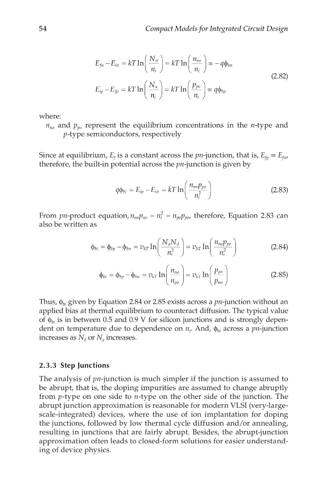
n no and p po represent the equilibrium concentrations in the n-type and
p-type semiconductors, respectively
Since at equilibrium, E f is a constant across the pn-junction, that is, E fp = E fn ,
therefore, the built-in potential across the pn-junction is given by
q
E E
kT
n p
n
bi
ip
in
n p
i
φ =
−
=
ln
o o
2
(2.83)
From pn-product equation, n p
n
n p
no no
i
p o po
= =
2
, therefore, Equation 2.83 can
also be written as
φ
φ
φ
bi
bp
bn
kT
a d
i
kT
no po
i
v
N N
n
v
n p
n
=
−
=
=
ln
ln
2
2
(2.84)
φ
φ
φ
bi
bp
bn
kT
no
po
kT
po
no
v
n
n
v
p
p
=
−
=
=
ln
ln
(2.85)
Thus, f bi given by Equation 2.84 or 2.85 exists across a pn-junction without an
applied bias at thermal equilibrium to counteract diffusion. The typical value
of f bi is in between 0.5 and 0.9 V for silicon junctions and is strongly dependent on temperature due to dependence on n i . And, f bi across a pn-junction
increases as N d or N a increases.
2.3.3 Step Junctions
The analysis of pn-junction is much simpler if the junction is assumed to
be abrupt, that is, the doping impurities are assumed to change abruptly
from p-type on one side to n-type on the other side of the junction. The
abrupt junction approximation is reasonable for modern VLSI (very-largescale-integrated) devices, where the use of ion implantation for doping
the junctions, followed by low thermal cycle diffusion and/or annealing,
resulting in junctions that are fairly abrupt. Besides, the abrupt-junction
approximation often leads to closed-form solutions for easier understanding of device physics.
Compact Models for Integrated Circuit Design
E E
kT
N
n
kT
n
n
q
E E
kT
N
fn
in
d
i
no
i
bn
ip
fp
a
−
=
=
≡ −
−
=
ln
ln
ln
φ
n n
kT
p
n
q
i
po
i
bp
=
≡
ln
φ
(2.82)
where:
n no and p po represent the equilibrium concentrations in the n-type and
p-type semiconductors, respectively
Since at equilibrium, E f is a constant across the pn-junction, that is, E fp = E fn ,
therefore, the built-in potential across the pn-junction is given by
q
E E
kT
n p
n
bi
ip
in
n p
i
φ =
−
=
ln
o o
2
(2.83)
From pn-product equation, n p
n
n p
no no
i
p o po
= =
2
, therefore, Equation 2.83 can
also be written as
φ
φ
φ
bi
bp
bn
kT
a d
i
kT
no po
i
v
N N
n
v
n p
n
=
−
=
=
ln
ln
2
2
(2.84)
φ
φ
φ
bi
bp
bn
kT
no
po
kT
po
no
v
n
n
v
p
p
=
−
=
=
ln
ln
(2.85)
Thus, f bi given by Equation 2.84 or 2.85 exists across a pn-junction without an
applied bias at thermal equilibrium to counteract diffusion. The typical value
of f bi is in between 0.5 and 0.9 V for silicon junctions and is strongly dependent on temperature due to dependence on n i . And, f bi across a pn-junction
increases as N d or N a increases.
2.3.3 Step Junctions
The analysis of pn-junction is much simpler if the junction is assumed to
be abrupt, that is, the doping impurities are assumed to change abruptly
from p-type on one side to n-type on the other side of the junction. The
abrupt junction approximation is reasonable for modern VLSI (very-largescale-integrated) devices, where the use of ion implantation for doping
the junctions, followed by low thermal cycle diffusion and/or annealing,
resulting in junctions that are fairly abrupt. Besides, the abrupt-junction
approximation often leads to closed-form solutions for easier understanding of device physics.