

53
Review of Basic Device Physics
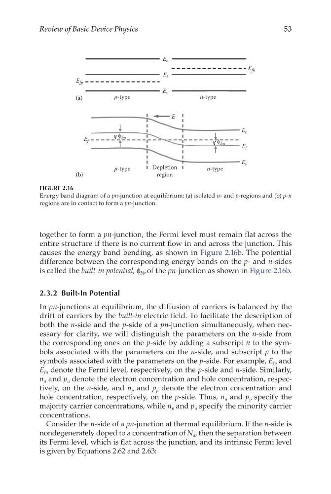
together to form a pn-junction, the Fermi level must remain flat across the
entire structure if there is no current flow in and across the junction. This
causes the energy band bending, as shown in Figure 2.16b. The potential
difference between the corresponding energy bands on the p- and n-sides
is called the built-in potential, f bi , of the pn-junction as shown in Figure 2.16b.
2.3.2 Built-In Potential
In pn-junctions at equilibrium, the diffusion of carriers is balanced by the
drift of carriers by the built-in electric field. To facilitate the description of
both the n-side and the p-side of a pn-junction simultaneously, when necessary for clarity, we will distinguish the parameters on the n-side from
the corresponding ones on the p-side by adding a subscript n to the symbols associated with the parameters on the n-side, and subscript p to the
symbols associated with the parameters on the p-side. For example, E fp and
E fn denote the Fermi level, respectively, on the p-side and n-side. Similarly,
n n and p n denote the electron concentration and hole concentration, respectively, on the n-side, and n p and p p denote the electron concentration and
hole concentration, respectively, on the p-side. Thus, n n and p p specify the
majority carrier concentrations, while n p and p n specify the minority carrier
concentrations.
Consider the n-side of a pn-junction at thermal equilibrium. If the n-side is
nondegenerately doped to a concentration of N d , then the separation between
its Fermi level, which is flat across the junction, and its intrinsic Fermi level
is given by Equations 2.62 and 2.63:
E c
E i
E fp
p-type
(a)
n-type
E fn
E v
(b)
p-type
n-type
E c
E i
E v
E
E f
q ϕ bp
−q ϕ bn
Depletion
region
FIGURE 2.16
Energy band diagram of a pn-junction at equilibrium: (a) isolated n- and p-regions and (b) p-n
regions are in contact to form a pn-junction.
Review of Basic Device Physics
together to form a pn-junction, the Fermi level must remain flat across the
entire structure if there is no current flow in and across the junction. This
causes the energy band bending, as shown in Figure 2.16b. The potential
difference between the corresponding energy bands on the p- and n-sides
is called the built-in potential, f bi , of the pn-junction as shown in Figure 2.16b.
2.3.2 Built-In Potential
In pn-junctions at equilibrium, the diffusion of carriers is balanced by the
drift of carriers by the built-in electric field. To facilitate the description of
both the n-side and the p-side of a pn-junction simultaneously, when necessary for clarity, we will distinguish the parameters on the n-side from
the corresponding ones on the p-side by adding a subscript n to the symbols associated with the parameters on the n-side, and subscript p to the
symbols associated with the parameters on the p-side. For example, E fp and
E fn denote the Fermi level, respectively, on the p-side and n-side. Similarly,
n n and p n denote the electron concentration and hole concentration, respectively, on the n-side, and n p and p p denote the electron concentration and
hole concentration, respectively, on the p-side. Thus, n n and p p specify the
majority carrier concentrations, while n p and p n specify the minority carrier
concentrations.
Consider the n-side of a pn-junction at thermal equilibrium. If the n-side is
nondegenerately doped to a concentration of N d , then the separation between
its Fermi level, which is flat across the junction, and its intrinsic Fermi level
is given by Equations 2.62 and 2.63:
E c
E i
E fp
p-type
(a)
n-type
E fn
E v
(b)
p-type
n-type
E c
E i
E v
E
E f
q ϕ bp
−q ϕ bn
Depletion
region
FIGURE 2.16
Energy band diagram of a pn-junction at equilibrium: (a) isolated n- and p-regions and (b) p-n
regions are in contact to form a pn-junction.