

438
Compact Models for Integrated Circuit Design
For MC simulation using ±3σ distribution for systematic variation and ±1σ
variation in mismatch, we can use the following commands in the HSPICE
netlist
.lib ‘lib’ MC
.param globalmismatchflag = 1
$ enable MC mismatch
.param globalsigmavtflag = 0
$ disable fixed V th mismatch
offset
.param globalmcflag = 1
$ enable MC systematic variation
Figure 12.6b shows the MC simulation results of IONN versus IONP for the
same CMOS technology. The corner values are shown for comparison only.
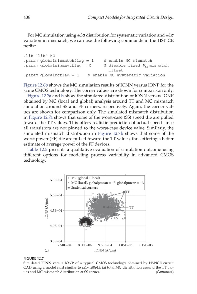
Figure 12.7a and b show the simulated distribution of IONN versus IONP
obtained by MC (local and global) analysis around TT and MC mismatch
simulation around SS and FF corners, respectively. Again, the corner values are shown for comparison only. The simulated mismatch distribution
in Figure 12.7a shows that some of the worst-case (SS) speed die are pulled
toward the TT values. This offers realistic prediction of actual speed since
all transistors are not pinned to the worst-case device value. Similarly, the
simulated mismatch distribution in Figure 12.7b shows that some of the
worst-power (FF) die are pulled toward the TT values, thus offering a better
estimate of average power of the FF devices.
Table 12.5 presents a qualitative evaluation of simulation outcome using
different options for modeling process variability in advanced CMOS
technology.
7.50E−04
3.5E−04
4.0E−04
4.5E−04
5.0E−04
5.5E−04
8.50E−04
MC (global + local)
Statistical corners
MC (local), globalpmean = −3, globalpmean = −3
FF
TT
SF
FS
SS
9.50E−04
IONN (A/μm)
(a)
IONP (A/μm)
1.15E−03
1.05E−03
FIGURE 12.7
Simulated IONN versus IONP of a typical CMOS technology obtained by HSPICE circuit
CAD using a model card similar to ex1mod0p1.l: (a) total MC distribution around the TT values and MC mismatch distribution at SS corner.
(Continued)
Compact Models for Integrated Circuit Design
For MC simulation using ±3σ distribution for systematic variation and ±1σ
variation in mismatch, we can use the following commands in the HSPICE
netlist
.lib ‘lib’ MC
.param globalmismatchflag = 1
$ enable MC mismatch
.param globalsigmavtflag = 0
$ disable fixed V th mismatch
offset
.param globalmcflag = 1
$ enable MC systematic variation
Figure 12.6b shows the MC simulation results of IONN versus IONP for the
same CMOS technology. The corner values are shown for comparison only.
Figure 12.7a and b show the simulated distribution of IONN versus IONP
obtained by MC (local and global) analysis around TT and MC mismatch
simulation around SS and FF corners, respectively. Again, the corner values are shown for comparison only. The simulated mismatch distribution
in Figure 12.7a shows that some of the worst-case (SS) speed die are pulled
toward the TT values. This offers realistic prediction of actual speed since
all transistors are not pinned to the worst-case device value. Similarly, the
simulated mismatch distribution in Figure 12.7b shows that some of the
worst-power (FF) die are pulled toward the TT values, thus offering a better
estimate of average power of the FF devices.
Table 12.5 presents a qualitative evaluation of simulation outcome using
different options for modeling process variability in advanced CMOS
technology.
7.50E−04
3.5E−04
4.0E−04
4.5E−04
5.0E−04
5.5E−04
8.50E−04
MC (global + local)
Statistical corners
MC (local), globalpmean = −3, globalpmean = −3
FF
TT
SF
FS
SS
9.50E−04
IONN (A/μm)
(a)
IONP (A/μm)
1.15E−03
1.05E−03
FIGURE 12.7
Simulated IONN versus IONP of a typical CMOS technology obtained by HSPICE circuit
CAD using a model card similar to ex1mod0p1.l: (a) total MC distribution around the TT values and MC mismatch distribution at SS corner.
(Continued)