

431
Compact Model Library for Circuit Simulation
variability-sensitive model parameters for corner modeling. Table 12.2 shows
a typical corner file for nMOSFETs with selected parameters to illustrate the
corner file generation technique.
In Table 12.2, TT defines the typical values of the extracted model parameters
at room temperature for NMOS and PMOS devices; SS, FF, SF, and FS define
the parameters for slow NMOS and slow PMOS, fast NMOS and fast PMOS,
slow NMOS and fast PMOS, and fast NMOS and slow PMOS, respectively, as
described in Chapter 8 [6,7]. It is to be noted that SS, FF, SF, and FS represent
the worst case speed (WS), worst case power (WP), worst case zero (WZ),
and worst case one (WO), respectively [6,7]. Each instance parameter (delta)
defines the variance of the corresponding model parameter. In Table 12.2,
0.00
0.20
0.40
0.60
0.30
0.90
0.60
1.00
0.80
1.00
1.4e−3
1.2e−3
1.0e−3
8.0e−4
6.0e−4
4.0e−4
0.0e+00
2.0e−4
V ds (V)
Max error = 4.38%
W/L/T = 1./2.6e-002/25. V bs = 0.00V:1:I d − V gs
RMS error = 2.34%
V gs (V) =
0.00
0.20
0.40
0.60
0.30
0.90
0.60
1.00
0.80
1.00
V ds (V)
Max error = 3.58%
W/L/T = 1./2.6e-002/25. V bs = 0.30V:2:I d − V gs
RMS error = 1.43%
V gs (V) =
1.2e−3
1.0e−3
8.0e−4
6.0e−4
4.0e−4
0.0e+00
2.0e−4
(e)
I
d (A)
(f )
I
d (A)
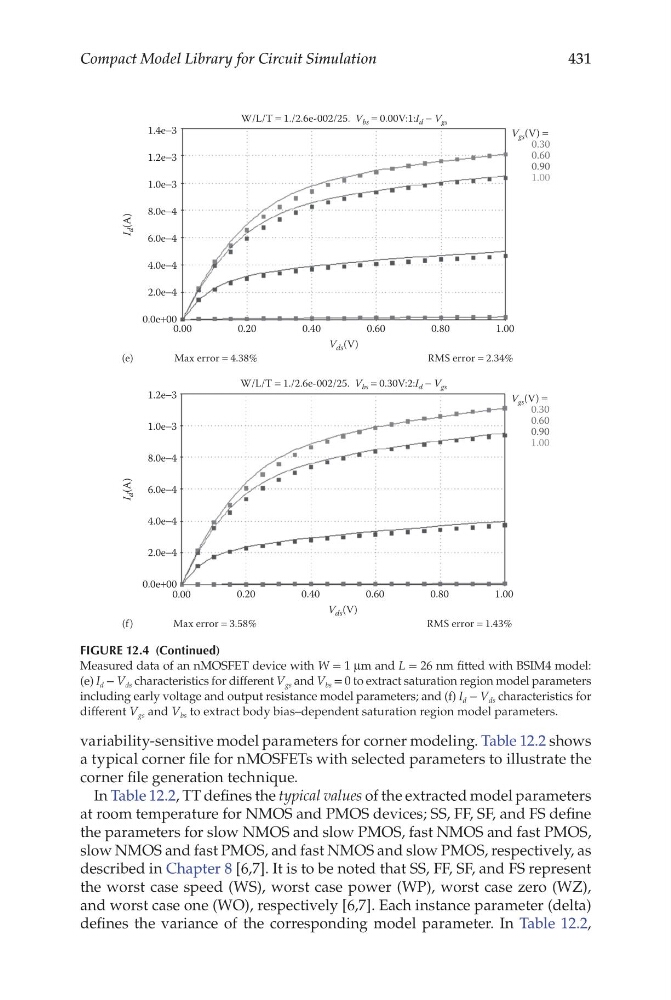
FIGURE 12.4 (Continued)
Measured data of an nMOSFET device with W = 1 μm and L = 26 nm fitted with BSIM4 model:
(e) I d − V ds characteristics for different V gs and V bs = 0 to extract saturation region model parameters
including early voltage and output resistance model parameters; and (f) I d − V ds characteristics for
different V gs and V bs to extract body bias–dependent saturation region model parameters.
Compact Model Library for Circuit Simulation
variability-sensitive model parameters for corner modeling. Table 12.2 shows
a typical corner file for nMOSFETs with selected parameters to illustrate the
corner file generation technique.
In Table 12.2, TT defines the typical values of the extracted model parameters
at room temperature for NMOS and PMOS devices; SS, FF, SF, and FS define
the parameters for slow NMOS and slow PMOS, fast NMOS and fast PMOS,
slow NMOS and fast PMOS, and fast NMOS and slow PMOS, respectively, as
described in Chapter 8 [6,7]. It is to be noted that SS, FF, SF, and FS represent
the worst case speed (WS), worst case power (WP), worst case zero (WZ),
and worst case one (WO), respectively [6,7]. Each instance parameter (delta)
defines the variance of the corresponding model parameter. In Table 12.2,
0.00
0.20
0.40
0.60
0.30
0.90
0.60
1.00
0.80
1.00
1.4e−3
1.2e−3
1.0e−3
8.0e−4
6.0e−4
4.0e−4
0.0e+00
2.0e−4
V ds (V)
Max error = 4.38%
W/L/T = 1./2.6e-002/25. V bs = 0.00V:1:I d − V gs
RMS error = 2.34%
V gs (V) =
0.00
0.20
0.40
0.60
0.30
0.90
0.60
1.00
0.80
1.00
V ds (V)
Max error = 3.58%
W/L/T = 1./2.6e-002/25. V bs = 0.30V:2:I d − V gs
RMS error = 1.43%
V gs (V) =
1.2e−3
1.0e−3
8.0e−4
6.0e−4
4.0e−4
0.0e+00
2.0e−4
(e)
I
d (A)
(f )
I
d (A)
FIGURE 12.4 (Continued)
Measured data of an nMOSFET device with W = 1 μm and L = 26 nm fitted with BSIM4 model:
(e) I d − V ds characteristics for different V gs and V bs = 0 to extract saturation region model parameters
including early voltage and output resistance model parameters; and (f) I d − V ds characteristics for
different V gs and V bs to extract body bias–dependent saturation region model parameters.