

419
Bipolar Junction Transistor Compact Models
b. Calculate the base-emitter forward bias V KF at which the high-level
injection is reached.
c. If the effect of high-level injection on the current gain β starts when
the injected minority-carrier density reaches 10% of the majority
carrier density, calculate the value of V BE at the onset of β roll-off
at high collector current level, I C .
d. Show the conditions obtained in part (b) and (c) on I C vs. V BE @
V BC = 0 characteristic of the transistor.
Define and label all parameters in your plot(s). Explain.
11.8 The SGP-BJT model, presented in this chapter, cannot model the
effect of parasitic substrate transistor on intrinsic devices. Consider
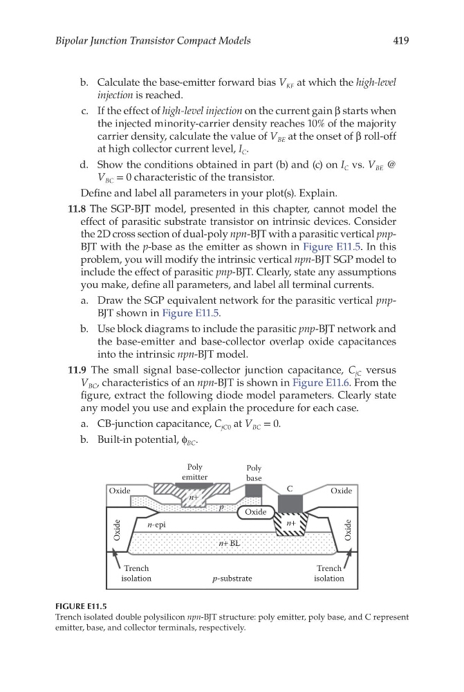
the 2D cross section of dual-poly npn-BJT with a parasitic vertical pnpBJT with the p-base as the emitter as shown in Figure E11.5. In this
problem, you will modify the intrinsic vertical npn-BJT SGP model to
include the effect of parasitic pnp-BJT. Clearly, state any assumptions
you make, define all parameters, and label all terminal currents.
a. Draw the SGP equivalent network for the parasitic vertical pnpBJT shown in Figure E11.5.
b. Use block diagrams to include the parasitic pnp-BJT network and
the base-emitter and base-collector overlap oxide capacitances
into the intrinsic npn-BJT model.
11.9 The small signal base-collector junction capacitance, C jC versus
V BC , characteristics of an npn-BJT is shown in Figure E11.6. From the
figure, extract the following diode model parameters. Clearly state
any model you use and explain the procedure for each case.
a. CB-junction capacitance, C jC0 at V BC = 0.
b. Built-in potential, f BC .
Trench
isolation
Poly
emitter
Poly
base
C
Trench
isolation
Oxide
Oxide
Oxide
Oxide
Oxide
n+
n+
n+ BL
n-epi
p
p-substrate
FIGURE E11.5
Trench isolated double polysilicon npn-BJT structure: poly emitter, poly base, and C represent
emitter, base, and collector terminals, respectively.
Bipolar Junction Transistor Compact Models
b. Calculate the base-emitter forward bias V KF at which the high-level
injection is reached.
c. If the effect of high-level injection on the current gain β starts when
the injected minority-carrier density reaches 10% of the majority
carrier density, calculate the value of V BE at the onset of β roll-off
at high collector current level, I C .
d. Show the conditions obtained in part (b) and (c) on I C vs. V BE @
V BC = 0 characteristic of the transistor.
Define and label all parameters in your plot(s). Explain.
11.8 The SGP-BJT model, presented in this chapter, cannot model the
effect of parasitic substrate transistor on intrinsic devices. Consider
the 2D cross section of dual-poly npn-BJT with a parasitic vertical pnpBJT with the p-base as the emitter as shown in Figure E11.5. In this
problem, you will modify the intrinsic vertical npn-BJT SGP model to
include the effect of parasitic pnp-BJT. Clearly, state any assumptions
you make, define all parameters, and label all terminal currents.
a. Draw the SGP equivalent network for the parasitic vertical pnpBJT shown in Figure E11.5.
b. Use block diagrams to include the parasitic pnp-BJT network and
the base-emitter and base-collector overlap oxide capacitances
into the intrinsic npn-BJT model.
11.9 The small signal base-collector junction capacitance, C jC versus
V BC , characteristics of an npn-BJT is shown in Figure E11.6. From the
figure, extract the following diode model parameters. Clearly state
any model you use and explain the procedure for each case.
a. CB-junction capacitance, C jC0 at V BC = 0.
b. Built-in potential, f BC .
Trench
isolation
Poly
emitter
Poly
base
C
Trench
isolation
Oxide
Oxide
Oxide
Oxide
Oxide
n+
n+
n+ BL
n-epi
p
p-substrate
FIGURE E11.5
Trench isolated double polysilicon npn-BJT structure: poly emitter, poly base, and C represent
emitter, base, and collector terminals, respectively.