

420
Compact Models for Integrated Circuit Design
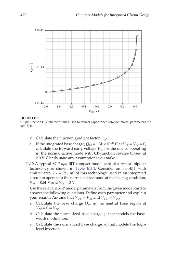
c. Calculate the junction gradient factor, m jC .
d. If the integrated base charge, Q B0 = 1.31 × 10 −12 C at V BE = V BC = 0,
calculate the forward early voltage V AF for the device operating
in the normal active mode with CB-junction reverse biased at
2.0 V. Clearly state any assumptions you make.
11.10 A typical SGP npn-BJT compact model card of a typical bipolar
technology is shown in Table E11.1. Consider an npn-BJT with
emitter area, A E = 25 μm 2 of this technology used in an integrated
circuit to operate in the normal active mode at the biasing condition,
V BE = 0.61 V and V CE = 3 V.
Use the relevant SGP model parameters from the given model card to
answer the following questions. Define each parameter and explain
your results. Assume that V B′E′ = V BE and V B′C′ = V BC .
a. Calculate the base charge Q B0 in the neutral base region at
V BE = 0 = V BC .
b. Calculate the normalized base charge q 1 that models the basewidth modulation.
c. Calculate the normalized base charge, q 2 that models the highlevel injection.
1.E−14
−2.0
−1.6
−1.2
−0.8
−0.4
0.0
0.4
0.8
1.E−13
1.E−12
C
jC (F)
V BC (V)
FIGURE E11.6
CB pn-junction C–V characteristics used to extract capacitance compact model parameters for
npn-BJTs.
Compact Models for Integrated Circuit Design
c. Calculate the junction gradient factor, m jC .
d. If the integrated base charge, Q B0 = 1.31 × 10 −12 C at V BE = V BC = 0,
calculate the forward early voltage V AF for the device operating
in the normal active mode with CB-junction reverse biased at
2.0 V. Clearly state any assumptions you make.
11.10 A typical SGP npn-BJT compact model card of a typical bipolar
technology is shown in Table E11.1. Consider an npn-BJT with
emitter area, A E = 25 μm 2 of this technology used in an integrated
circuit to operate in the normal active mode at the biasing condition,
V BE = 0.61 V and V CE = 3 V.
Use the relevant SGP model parameters from the given model card to
answer the following questions. Define each parameter and explain
your results. Assume that V B′E′ = V BE and V B′C′ = V BC .
a. Calculate the base charge Q B0 in the neutral base region at
V BE = 0 = V BC .
b. Calculate the normalized base charge q 1 that models the basewidth modulation.
c. Calculate the normalized base charge, q 2 that models the highlevel injection.
1.E−14
−2.0
−1.6
−1.2
−0.8
−0.4
0.0
0.4
0.8
1.E−13
1.E−12
C
jC (F)
V BC (V)
FIGURE E11.6
CB pn-junction C–V characteristics used to extract capacitance compact model parameters for
npn-BJTs.