

418
Compact Models for Integrated Circuit Design
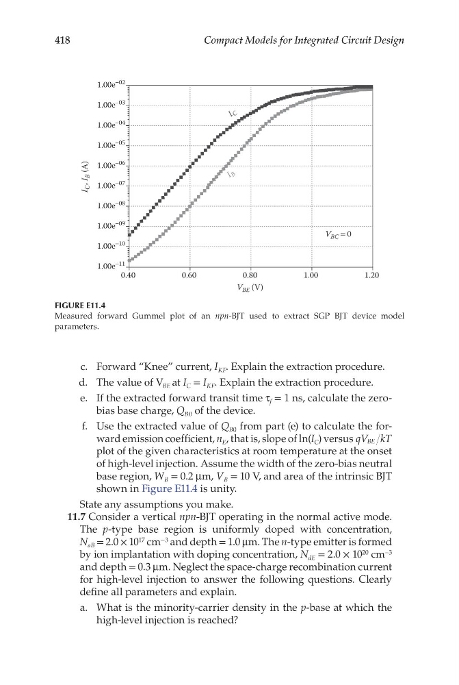
c. Forward “Knee” current, I KF . Explain the extraction procedure.
d. The value of V BE at I C = I KF . Explain the extraction procedure.
e. If the extracted forward transit time τ f = 1 ns, calculate the zerobias base charge, Q B0 of the device.
f. Use the extracted value of Q B0 from part (e) to calculate the forward emission coefficient, n E , that is, slope of ln(I C ) versus qV kT
BE
plot of the given characteristics at room temperature at the onset
of high-level injection. Assume the width of the zero-bias neutral
base region, W B = 0.2 μm, V B = 10 V, and area of the intrinsic BJT
shown in Figure E11.4 is unity.
State any assumptions you make.
11.7 Consider a vertical npn-BJT operating in the normal active mode.
The p-type base region is uniformly doped with concentration,
N aB = 2.0 × 10 17 cm −3 and depth = 1.0 μm. The n-type emitter is formed
by ion implantation with doping concentration, N dE = 2.0 × 10 20 cm −3
and depth = 0.3 μm. Neglect the space-charge recombination current
for high-level injection to answer the following questions. Clearly
define all parameters and explain.
a. What is the minority-carrier density in the p-base at which the
high-level injection is reached?
1.00e
−02
1.00e
−03
1.00e
−04
1.00e
−05
1.00e
−06
1.00e
−07
1.00e
−08
1.00e
−09
1.00e
−10
1.00e
−11
I
C , I
B (A)
0.40
V BE (V)
V BC = 0
0.60
0.80
1.00
1.20
I C
I B
FIGURE E11.4
Measured forward Gummel plot of an npn-BJT used to extract SGP BJT device model
parameters.
Compact Models for Integrated Circuit Design
c. Forward “Knee” current, I KF . Explain the extraction procedure.
d. The value of V BE at I C = I KF . Explain the extraction procedure.
e. If the extracted forward transit time τ f = 1 ns, calculate the zerobias base charge, Q B0 of the device.
f. Use the extracted value of Q B0 from part (e) to calculate the forward emission coefficient, n E , that is, slope of ln(I C ) versus qV kT
BE
plot of the given characteristics at room temperature at the onset
of high-level injection. Assume the width of the zero-bias neutral
base region, W B = 0.2 μm, V B = 10 V, and area of the intrinsic BJT
shown in Figure E11.4 is unity.
State any assumptions you make.
11.7 Consider a vertical npn-BJT operating in the normal active mode.
The p-type base region is uniformly doped with concentration,
N aB = 2.0 × 10 17 cm −3 and depth = 1.0 μm. The n-type emitter is formed
by ion implantation with doping concentration, N dE = 2.0 × 10 20 cm −3
and depth = 0.3 μm. Neglect the space-charge recombination current
for high-level injection to answer the following questions. Clearly
define all parameters and explain.
a. What is the minority-carrier density in the p-base at which the
high-level injection is reached?
1.00e
−02
1.00e
−03
1.00e
−04
1.00e
−05
1.00e
−06
1.00e
−07
1.00e
−08
1.00e
−09
1.00e
−10
1.00e
−11
I
C , I
B (A)
0.40
V BE (V)
V BC = 0
0.60
0.80
1.00
1.20
I C
I B
FIGURE E11.4
Measured forward Gummel plot of an npn-BJT used to extract SGP BJT device model
parameters.