

417
Bipolar Junction Transistor Compact Models
11.4 Consider an npn-BJT in the inverse active mode of operation in
the high-level injection regime. For simplicity of modeling, you can
assume uniformly doped base region.
a. Schematically show the components of base charge, Q B , under
the above operating condition. Label your plot and show the
integration limits to compute different components of Q B .
b. Write down the expression for the normalized base-charge
responsible for base-width modulation in terms of junction biases
and early voltages. Define all parameters and explain.
c. Write down the expression for SGP-model current source for basewidth modulation in terms of early voltages only under the above
specified operating condition. Define all parameters and explain.
11.5 The Gummel plot shown in Figure 11.20 for npn-BJT is obtained
at V BC = 0 and is used for DC compact model parameter extraction.
a. Describe graphically how I C versus V BE characteristics at V BC = 0
can be obtained from I C versus V CE characteristics at different V BE
for an npn-BJT.
b. Mathematically describe the methodology to extract BJT saturation current I SS for I C − V BE plot at V BC = 0.
Clearly define any assumptions you make.
11.6 The measured forward Gummel-plot of an npn-BJT is shown in
Figure E11.4. Extract the following SGP-model parameters.
a. BJT saturation current, I SS . Explain the extraction procedure.
b. Maximum forward current gain, β FM . Explain the extraction
procedure.
p-Substrate
n+
n−
n+
p+
p+
p
B
E
C
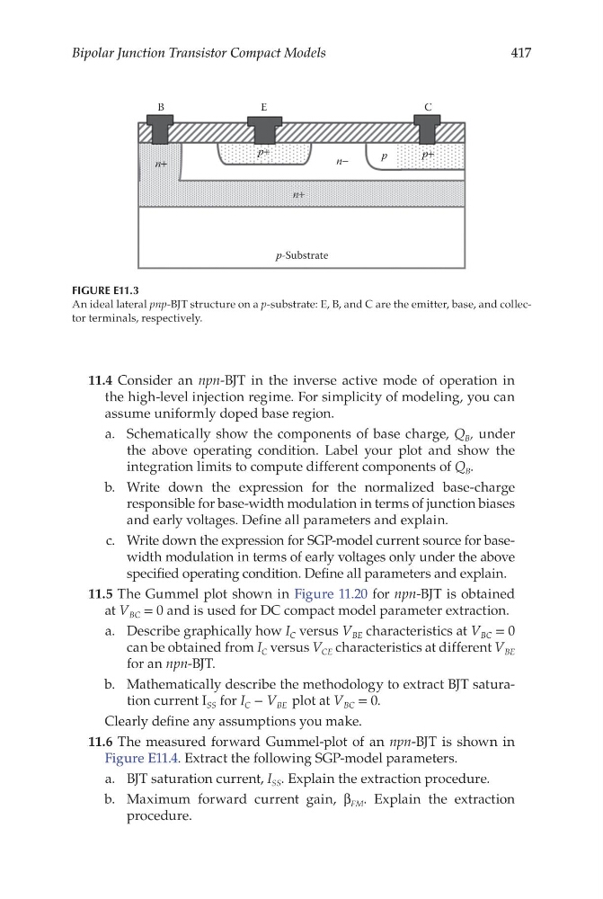
FIGURE E11.3
An ideal lateral pnp-BJT structure on a p-substrate: E, B, and C are the emitter, base, and collector terminals, respectively.
Bipolar Junction Transistor Compact Models
11.4 Consider an npn-BJT in the inverse active mode of operation in
the high-level injection regime. For simplicity of modeling, you can
assume uniformly doped base region.
a. Schematically show the components of base charge, Q B , under
the above operating condition. Label your plot and show the
integration limits to compute different components of Q B .
b. Write down the expression for the normalized base-charge
responsible for base-width modulation in terms of junction biases
and early voltages. Define all parameters and explain.
c. Write down the expression for SGP-model current source for basewidth modulation in terms of early voltages only under the above
specified operating condition. Define all parameters and explain.
11.5 The Gummel plot shown in Figure 11.20 for npn-BJT is obtained
at V BC = 0 and is used for DC compact model parameter extraction.
a. Describe graphically how I C versus V BE characteristics at V BC = 0
can be obtained from I C versus V CE characteristics at different V BE
for an npn-BJT.
b. Mathematically describe the methodology to extract BJT saturation current I SS for I C − V BE plot at V BC = 0.
Clearly define any assumptions you make.
11.6 The measured forward Gummel-plot of an npn-BJT is shown in
Figure E11.4. Extract the following SGP-model parameters.
a. BJT saturation current, I SS . Explain the extraction procedure.
b. Maximum forward current gain, β FM . Explain the extraction
procedure.
p-Substrate
n+
n−
n+
p+
p+
p
B
E
C
FIGURE E11.3
An ideal lateral pnp-BJT structure on a p-substrate: E, B, and C are the emitter, base, and collector terminals, respectively.