

398
Compact Models for Integrated Circuit Design
Using assumption 1, we can use 1D expression for the electron and hole
current densities (Equations 2.76 and 2.77) as
J q n x E x qD
dn
dx
J q p x E x qD
dp
dx
n
n
n
p
p
p
=
+
=
−
µ
µ
( ) ( )
( ) ( )
(electrons)
(hol les)
(11.53)
Now from assumption 4, for a high-gain npn-BJT, I B ≅ 0, that is, the hole current ≅ 0; then from the hole current expression J p in Equation 11.53, we get
0 =
−
q p x E x qD
dp
dx
p
p
µ ( ) ( )
(11.54)
After simplification of Equation 11.54 and using Equation 2.42, we can show
that the built-in electric field E(x) due to nonuniform base doping of npn-BJTs
is given by (Equation 2.46)
E x
D
p x
dp
dx
v p x
dp
dx
p
p
kT
( )
( )
( )
=
=
µ
1
1
(11.55)
The direction of the electric field E(x) in Equation 11.55 aids the electron flow
from the emitter to collector and retards the electron flow from the collector
to emitter. Now, the flow of electrons from the emitter to collector is given
by the electron current expression J n in Equation 11.53. Then, substituting for
E(x) from Equation 11.55 to Equation 11.53 we get
J q n x v p x
dp x
dx
qD
dn
dx
n
n
kT
n
=
+
µ ( )
( )
( )
1
(11.56)
EB spacecharge
region
E
CB spacecharge
region
B
C
X jE
X jC
x E
x C
p(x)
n(x)
E(x)
x
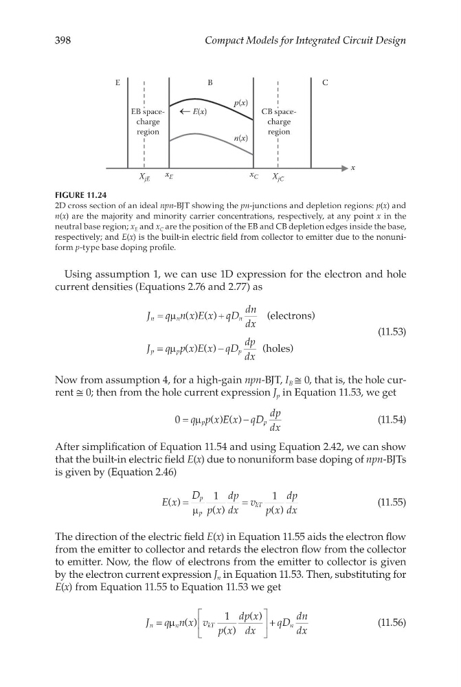
FIGURE 11.24
2D cross section of an ideal npn-BJT showing the pn-junctions and depletion regions: p(x) and
n(x) are the majority and minority carrier concentrations, respectively, at any point x in the
neutral base region; x E and x C are the position of the EB and CB depletion edges inside the base,
respectively; and E(x) is the built-in electric field from collector to emitter due to the nonuniform p-type base doping profile.
Compact Models for Integrated Circuit Design
Using assumption 1, we can use 1D expression for the electron and hole
current densities (Equations 2.76 and 2.77) as
J q n x E x qD
dn
dx
J q p x E x qD
dp
dx
n
n
n
p
p
p
=
+
=
−
µ
µ
( ) ( )
( ) ( )
(electrons)
(hol les)
(11.53)
Now from assumption 4, for a high-gain npn-BJT, I B ≅ 0, that is, the hole current ≅ 0; then from the hole current expression J p in Equation 11.53, we get
0 =
−
q p x E x qD
dp
dx
p
p
µ ( ) ( )
(11.54)
After simplification of Equation 11.54 and using Equation 2.42, we can show
that the built-in electric field E(x) due to nonuniform base doping of npn-BJTs
is given by (Equation 2.46)
E x
D
p x
dp
dx
v p x
dp
dx
p
p
kT
( )
( )
( )
=
=
µ
1
1
(11.55)
The direction of the electric field E(x) in Equation 11.55 aids the electron flow
from the emitter to collector and retards the electron flow from the collector
to emitter. Now, the flow of electrons from the emitter to collector is given
by the electron current expression J n in Equation 11.53. Then, substituting for
E(x) from Equation 11.55 to Equation 11.53 we get
J q n x v p x
dp x
dx
qD
dn
dx
n
n
kT
n
=
+
µ ( )
( )
( )
1
(11.56)
EB spacecharge
region
E
CB spacecharge
region
B
C
X jE
X jC
x E
x C
p(x)
n(x)
E(x)
x
FIGURE 11.24
2D cross section of an ideal npn-BJT showing the pn-junctions and depletion regions: p(x) and
n(x) are the majority and minority carrier concentrations, respectively, at any point x in the
neutral base region; x E and x C are the position of the EB and CB depletion edges inside the base,
respectively; and E(x) is the built-in electric field from collector to emitter due to the nonuniform p-type base doping profile.