

397
Bipolar Junction Transistor Compact Models
significantly and, therefore, must be modeled for accurate simulation of BJTs
in circuit CAD.
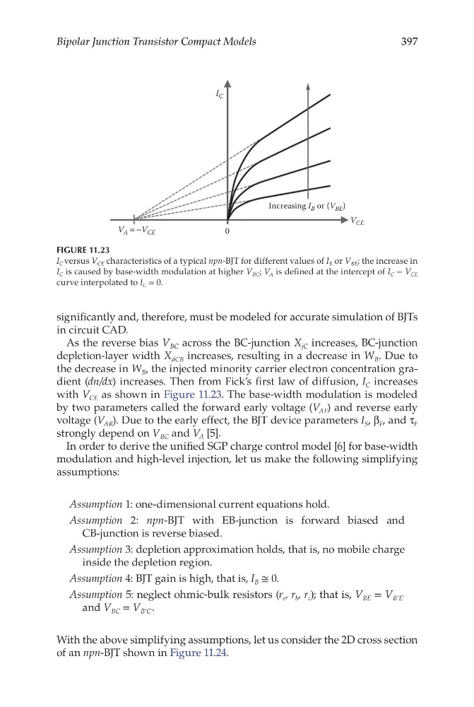
As the reverse bias V BC across the BC-junction X jC increases, BC-junction
depletion-layer width X dCB increases, resulting in a decrease in W B . Due to
the decrease in W B , the injected minority carrier electron concentration gradient (dn/dx) increases. Then from Fick’s first law of diffusion, I C increases
with V CE as shown in Figure 11.23. The base-width modulation is modeled
by two parameters called the forward early voltage (V AF ) and reverse early
voltage (V AR ). Due to the early effect, the BJT device parameters I S , β F , and τ F
strongly depend on V BC and V A [5].
In order to derive the unified SGP charge control model [6] for base-width
modulation and high-level injection, let us make the following simplifying
assumptions:
Assumption 1: one-dimensional current equations hold.
Assumption 2: npn-BJT with EB-junction is forward biased and
CB-junction is reverse biased.
Assumption 3: depletion approximation holds, that is, no mobile charge
inside the depletion region.
Assumption 4: BJT gain is high, that is, I B ≅ 0.
Assumption 5: neglect ohmic-bulk resistors (r e , r b , r c ); that is, V BE = V B′E′
and V BC = V B′C′ .
With the above simplifying assumptions, let us consider the 2D cross section
of an npn-BJT shown in Figure 11.24.
I C
V CE
V A = −V CE
Increasing I B or (V BE )
0
FIGURE 11.23
I C versus V CE characteristics of a typical npn-BJT for different values of I B or V BE ; the increase in
I C is caused by base-width modulation at higher V BC ; V A is defined at the intercept of I C − V CE
curve interpolated to I C = 0.
Bipolar Junction Transistor Compact Models
significantly and, therefore, must be modeled for accurate simulation of BJTs
in circuit CAD.
As the reverse bias V BC across the BC-junction X jC increases, BC-junction
depletion-layer width X dCB increases, resulting in a decrease in W B . Due to
the decrease in W B , the injected minority carrier electron concentration gradient (dn/dx) increases. Then from Fick’s first law of diffusion, I C increases
with V CE as shown in Figure 11.23. The base-width modulation is modeled
by two parameters called the forward early voltage (V AF ) and reverse early
voltage (V AR ). Due to the early effect, the BJT device parameters I S , β F , and τ F
strongly depend on V BC and V A [5].
In order to derive the unified SGP charge control model [6] for base-width
modulation and high-level injection, let us make the following simplifying
assumptions:
Assumption 1: one-dimensional current equations hold.
Assumption 2: npn-BJT with EB-junction is forward biased and
CB-junction is reverse biased.
Assumption 3: depletion approximation holds, that is, no mobile charge
inside the depletion region.
Assumption 4: BJT gain is high, that is, I B ≅ 0.
Assumption 5: neglect ohmic-bulk resistors (r e , r b , r c ); that is, V BE = V B′E′
and V BC = V B′C′ .
With the above simplifying assumptions, let us consider the 2D cross section
of an npn-BJT shown in Figure 11.24.
I C
V CE
V A = −V CE
Increasing I B or (V BE )
0
FIGURE 11.23
I C versus V CE characteristics of a typical npn-BJT for different values of I B or V BE ; the increase in
I C is caused by base-width modulation at higher V BC ; V A is defined at the intercept of I C − V CE
curve interpolated to I C = 0.