

396
Compact Models for Integrated Circuit Design
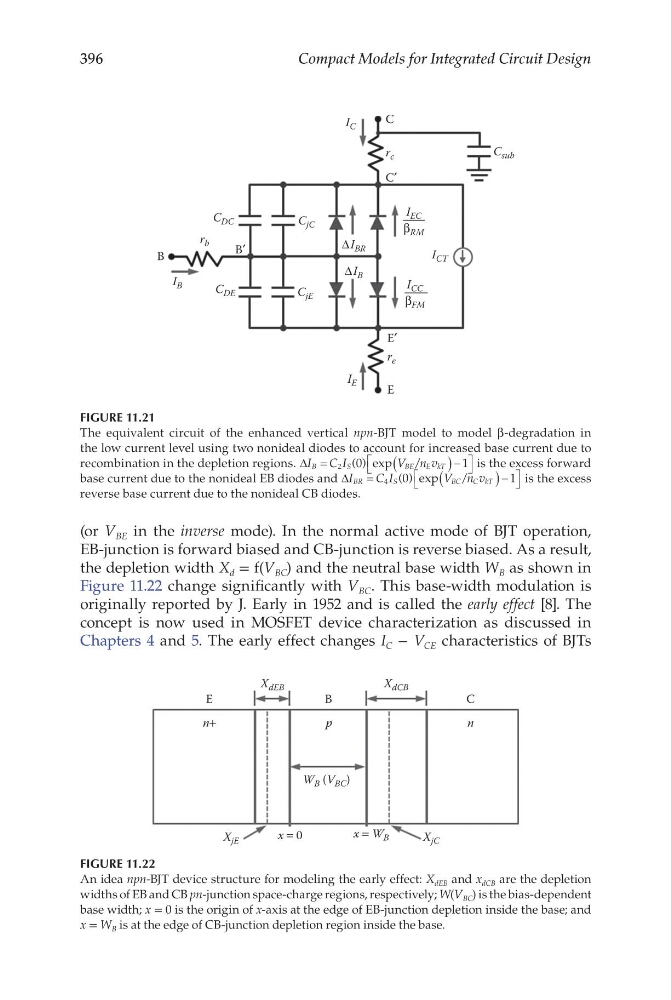
(or V BE in the inverse mode). In the normal active mode of BJT operation,
EB-junction is forward biased and CB-junction is reverse biased. As a result,
the depletion width X d = f(V BC ) and the neutral base width W B as shown in
Figure 11.22 change significantly with V BC . This base-width modulation is
originally reported by J. Early in 1952 and is called the early effect [8]. The
concept is now used in MOSFET device characterization as discussed in
Chapters 4 and 5. The early effect changes I C − V CE characteristics of BJTs
C
E
B
X dEB
X jE
X jC
X dCB
n+
n
p
W B (V BC )
x = 0
x = W B
FIGURE 11.22
An idea npn-BJT device structure for modeling the early effect: X dEB and x dCB are the depletion
widths of EB and CB pn-junction space-charge regions, respectively; W(V BC ) is the bias- dependent
base width; x = 0 is the origin of x-axis at the edge of EB-junction depletion inside the base; and
x = W B is at the edge of CB-junction depletion region inside the base.
E′
C′
B′
C
E
B
r c
C sub
r b
r e
C jE
C jC
C DE
C DC
I B
I C
I E
I CT
I EC
β RM
I CC
β FM
Δ I BR
Δ I B
FIGURE 11.21
The equivalent circuit of the enhanced vertical npn-BJT model to model β-degradation in
the low current level using two nonideal diodes to account for increased base current due to
recombination in the depletion regions. ∆I C I
V n v
B
S
BE
E kT
=
(
)−
2
0
1
( ) exp
/
is the excess forward
base current due to the nonideal EB diodes and ∆I
C I
V n v
BR
S
k T
=
(
)−
4
0
1
( ) exp
/
BC
C
is the excess
reverse base current due to the nonideal CB diodes.
Compact Models for Integrated Circuit Design
(or V BE in the inverse mode). In the normal active mode of BJT operation,
EB-junction is forward biased and CB-junction is reverse biased. As a result,
the depletion width X d = f(V BC ) and the neutral base width W B as shown in
Figure 11.22 change significantly with V BC . This base-width modulation is
originally reported by J. Early in 1952 and is called the early effect [8]. The
concept is now used in MOSFET device characterization as discussed in
Chapters 4 and 5. The early effect changes I C − V CE characteristics of BJTs
C
E
B
X dEB
X jE
X jC
X dCB
n+
n
p
W B (V BC )
x = 0
x = W B
FIGURE 11.22
An idea npn-BJT device structure for modeling the early effect: X dEB and x dCB are the depletion
widths of EB and CB pn-junction space-charge regions, respectively; W(V BC ) is the bias- dependent
base width; x = 0 is the origin of x-axis at the edge of EB-junction depletion inside the base; and
x = W B is at the edge of CB-junction depletion region inside the base.
E′
C′
B′
C
E
B
r c
C sub
r b
r e
C jE
C jC
C DE
C DC
I B
I C
I E
I CT
I EC
β RM
I CC
β FM
Δ I BR
Δ I B
FIGURE 11.21
The equivalent circuit of the enhanced vertical npn-BJT model to model β-degradation in
the low current level using two nonideal diodes to account for increased base current due to
recombination in the depletion regions. ∆I C I
V n v
B
S
BE
E kT
=
(
)−
2
0
1
( ) exp
/
is the excess forward
base current due to the nonideal EB diodes and ∆I
C I
V n v
BR
S
k T
=
(
)−
4
0
1
( ) exp
/
BC
C
is the excess
reverse base current due to the nonideal CB diodes.