

394
Compact Models for Integrated Circuit Design
It is observed from Figure 11.20 that the β-degradation at low current level
is due to the increase in the base current, whereas β-roll-off at high current condition is due to the decrease in the collector current. The observed
β-degradation at low current level is attributed to the recombination of
injected carriers in the space-charge regions whereas β-roll-off at high current condition is due to the high-level injection.
Thus, in order to improve the simulation accuracy, we will develop models
for minority carrier recombination in the space-charge regions, base-width
modulation, and high-level injection to include in the BJT model described
in Figure 11.13. First of all, we will develop models for the minority carrier
recombination in the EB and CB pn-junction depletion regions and include in
the model shown in Figure 11.13. Finally, we will include models for the basewidth modulation and high-level injection and present a complete compact
BJT model for circuit CAD.
11.5.3 Modeling Carrier Recombination in the Depletion Regions
In Region I of Figure 11.20, the increase in I B is due to the minority carrier
recombination in the EB and CB pn-junction depletion regions. For the simplicity of analysis, we assume a vertical npn-BJT in the normal active mode
of operation and neglect the ohmic-bulk resistors (r e , r b , r c ) so that V BE = V B'E'
and V BC = V B'C' .
Let us consider the effect of the minority carrier recombination in the
EB-depletion region only by setting V BC = 0. In Region I, the decrease in β
can be modeled by additional components of I B from
• Carrier recombination at the surface, I B (surface)
• Carrier recombination in the EB space-charge layer, I B (EB-scl)
• EB surface channels, I B (channel)
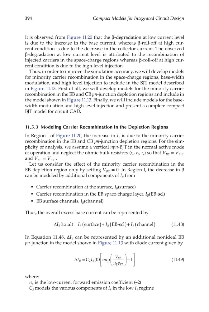
Thus, the overall excess base current can be represented by
∆I
I
I
I
B
B
B
B
(
)
total
surface
EB-scl
channel
= (
)+ (
)+ (
)
(11.48)
In Equation 11.48, ΔI B can be represented by an additional nonideal EB
pn-junction in the model shown in Figure 11.13 with diode current given by
∆I C I
V
n v
B
S
BE
E kT
=
−
2
0
1
( ) exp
(11.49)
where:
n E is the low-current forward emission coefficient (~2)
C 2 models the various components of I S in the low I B regime
Compact Models for Integrated Circuit Design
It is observed from Figure 11.20 that the β-degradation at low current level
is due to the increase in the base current, whereas β-roll-off at high current condition is due to the decrease in the collector current. The observed
β-degradation at low current level is attributed to the recombination of
injected carriers in the space-charge regions whereas β-roll-off at high current condition is due to the high-level injection.
Thus, in order to improve the simulation accuracy, we will develop models
for minority carrier recombination in the space-charge regions, base-width
modulation, and high-level injection to include in the BJT model described
in Figure 11.13. First of all, we will develop models for the minority carrier
recombination in the EB and CB pn-junction depletion regions and include in
the model shown in Figure 11.13. Finally, we will include models for the basewidth modulation and high-level injection and present a complete compact
BJT model for circuit CAD.
11.5.3 Modeling Carrier Recombination in the Depletion Regions
In Region I of Figure 11.20, the increase in I B is due to the minority carrier
recombination in the EB and CB pn-junction depletion regions. For the simplicity of analysis, we assume a vertical npn-BJT in the normal active mode
of operation and neglect the ohmic-bulk resistors (r e , r b , r c ) so that V BE = V B'E'
and V BC = V B'C' .
Let us consider the effect of the minority carrier recombination in the
EB-depletion region only by setting V BC = 0. In Region I, the decrease in β
can be modeled by additional components of I B from
• Carrier recombination at the surface, I B (surface)
• Carrier recombination in the EB space-charge layer, I B (EB-scl)
• EB surface channels, I B (channel)
Thus, the overall excess base current can be represented by
∆I
I
I
I
B
B
B
B
(
)
total
surface
EB-scl
channel
= (
)+ (
)+ (
)
(11.48)
In Equation 11.48, ΔI B can be represented by an additional nonideal EB
pn-junction in the model shown in Figure 11.13 with diode current given by
∆I C I
V
n v
B
S
BE
E kT
=
−
2
0
1
( ) exp
(11.49)
where:
n E is the low-current forward emission coefficient (~2)
C 2 models the various components of I S in the low I B regime