

385
Bipolar Junction Transistor Compact Models
the basic model by including the parasitic resistances and the capacitances to
enable transient analysis and improve DC modeling accuracy. This updated
EM1 model is often referred to as the EM2 BJT model and is described in the
following section.
11.5.2 Enhancement of the Basic Model
11.5.2.1 Modeling Parasitic Circuit Elements
The basic BJT model is extended to improve DC modeling accuracy and
enable transient simulation by including parasitic circuit elements in BJT
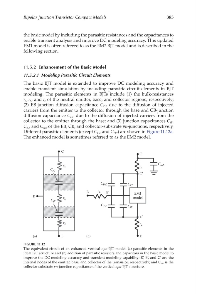
modeling. The parasitic elements in BJTs include (1) the bulk-resistances
r r
e b
, , and r c of the neutral emitter, base, and collector regions, respectively;
(2) EB-junction diffusion capacitance C DE due to the diffusion of injected
carriers from the emitter to the collector through the base and CB-junction
diffusion capacitance C DC due to the diffusion of injected carriers from the
collector to the emitter through the base; and (3) junction capacitances C jE ,
C jC , and C sub of the EB, CB, and collector-substrate pn-junctions, respectively.
Different parasitic elements (except C DE and C DC ) are shown in Figure 11.12a.
The enhanced model is sometimes referred to as the EM2 model.
E′
C′
B′
C
EM1
model
C
E
E
B
(a)
(b)
B
r c
r c
C sub
r b
r b
r e
r e
C jC
C jE
C jC
C DE
C DC
C jE
FIGURE 11.12
The equivalent circuit of an enhanced vertical npn-BJT model: (a) parasitic elements in the
ideal BJT structure and (b) addition of parasitic resistors and capacitors in the basic model to
improve the DC modeling accuracy and transient modeling capability; E′, B′, and C′ are the
internal nodes of the emitter, base, and collector of the transistor, respectively; and C sub is the
collector-substrate pn-junction capacitance of the vertical npn-BJT structure.
Bipolar Junction Transistor Compact Models
the basic model by including the parasitic resistances and the capacitances to
enable transient analysis and improve DC modeling accuracy. This updated
EM1 model is often referred to as the EM2 BJT model and is described in the
following section.
11.5.2 Enhancement of the Basic Model
11.5.2.1 Modeling Parasitic Circuit Elements
The basic BJT model is extended to improve DC modeling accuracy and
enable transient simulation by including parasitic circuit elements in BJT
modeling. The parasitic elements in BJTs include (1) the bulk-resistances
r r
e b
, , and r c of the neutral emitter, base, and collector regions, respectively;
(2) EB-junction diffusion capacitance C DE due to the diffusion of injected
carriers from the emitter to the collector through the base and CB-junction
diffusion capacitance C DC due to the diffusion of injected carriers from the
collector to the emitter through the base; and (3) junction capacitances C jE ,
C jC , and C sub of the EB, CB, and collector-substrate pn-junctions, respectively.
Different parasitic elements (except C DE and C DC ) are shown in Figure 11.12a.
The enhanced model is sometimes referred to as the EM2 model.
E′
C′
B′
C
EM1
model
C
E
E
B
(a)
(b)
B
r c
r c
C sub
r b
r b
r e
r e
C jC
C jE
C jC
C DE
C DC
C jE
FIGURE 11.12
The equivalent circuit of an enhanced vertical npn-BJT model: (a) parasitic elements in the
ideal BJT structure and (b) addition of parasitic resistors and capacitors in the basic model to
improve the DC modeling accuracy and transient modeling capability; E′, B′, and C′ are the
internal nodes of the emitter, base, and collector of the transistor, respectively; and C sub is the
collector-substrate pn-junction capacitance of the vertical npn-BJT structure.