

386
Compact Models for Integrated Circuit Design
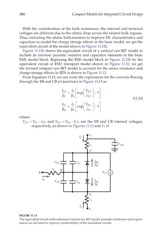
With the consideration of the bulk resistances, the internal and terminal
voltages are different due to the ohmic drop across the neutral bulk regions.
Thus, including the ohmic bulk-resistors to improve DC characteristics and
capacitors to model the charge storage effects in the basic model, we get the
equivalent circuit of the model shown in Figure 11.12b.
Figure 11.12b shows the equivalent circuit of a vertical npn-BJT model to
include its intrinsic parasitic resistive and capacitive elements in the basic
EM1 model block. Replacing the EM1 model block in Figure 11.12b by the
equivalent circuit of EM1 transport model shown in Figure 11.10, we get
the revised compact npn-BJT model to account for the series resistance and
charge storage effects in BJTs is shown in Figure 11.13.
From Equation 11.13, we can write the expressions for the currents flowing
through the EB and CB pn-junctions in Figure 11.13 as
I
I
V
v
I
I
V
v
CC
F
S
F
B E
kT
EC
R
S
R
B C
kT
β
β
β
β
=
−
=
′ ′
′ ′
exp
exp
1
−
1
(11.33)
where:
V
V
I r
B E
BE
E e
′ ′ =
−
and V
V
I r
B C
BC
C c
′ ′ =
−
are the EB and CB internal voltages,
respectively, as shown in Figures 11.13 and 11.14
E′
C′
B′
C
E
B
r c
C sub
r b
r e
C jE
C jC
C DE
C DC
I B
I C
I E
I CT
I EC
β R
I CC
β F
FIGURE 11.13
The equivalent circuit of the enhanced vertical npn-BJT model: parasitic resistances and capacitances are included to improve predictability of the simulation results.
Compact Models for Integrated Circuit Design
With the consideration of the bulk resistances, the internal and terminal
voltages are different due to the ohmic drop across the neutral bulk regions.
Thus, including the ohmic bulk-resistors to improve DC characteristics and
capacitors to model the charge storage effects in the basic model, we get the
equivalent circuit of the model shown in Figure 11.12b.
Figure 11.12b shows the equivalent circuit of a vertical npn-BJT model to
include its intrinsic parasitic resistive and capacitive elements in the basic
EM1 model block. Replacing the EM1 model block in Figure 11.12b by the
equivalent circuit of EM1 transport model shown in Figure 11.10, we get
the revised compact npn-BJT model to account for the series resistance and
charge storage effects in BJTs is shown in Figure 11.13.
From Equation 11.13, we can write the expressions for the currents flowing
through the EB and CB pn-junctions in Figure 11.13 as
I
I
V
v
I
I
V
v
CC
F
S
F
B E
kT
EC
R
S
R
B C
kT
β
β
β
β
=
−
=
′ ′
′ ′
exp
exp
1
−
1
(11.33)
where:
V
V
I r
B E
BE
E e
′ ′ =
−
and V
V
I r
B C
BC
C c
′ ′ =
−
are the EB and CB internal voltages,
respectively, as shown in Figures 11.13 and 11.14
E′
C′
B′
C
E
B
r c
C sub
r b
r e
C jE
C jC
C DE
C DC
I B
I C
I E
I CT
I EC
β R
I CC
β F
FIGURE 11.13
The equivalent circuit of the enhanced vertical npn-BJT model: parasitic resistances and capacitances are included to improve predictability of the simulation results.