

384
Compact Models for Integrated Circuit Design
Applying the chain rule and substituting the small signal current gain from
Equation 11.27, we find that
1
r
i
v
i
i
i
v
g
B
BE Q
B
C Q
C
BE Q
m
F
π
β
=
∂
∂
=
∂
∂
∂
∂
=
(11.30)
where we identified the transconductance g m from Equation 11.22. Substituting
for g m from Equation 11.24 at the operating point Q, we find the input resistance is
r
v
I
g
F kT
C
F
m
π
β
β
=
=
(11.31)
From Equation 11.31, it is obvious that the input resistance of BJTs is inversely
proportional to the DC collector current I C and directly proportional to the
small signal current gain β F .
Output resistance: In the normal active mode of operation, the CB-junction
is reverse biased. Therefore, the output resistance of the reverse-biased pnjunction is defined by
1
r
i
v
g
o
C
CE Q
o
=
∂
∂
≡
(11.32)
where:
g o is the output conductance of the device
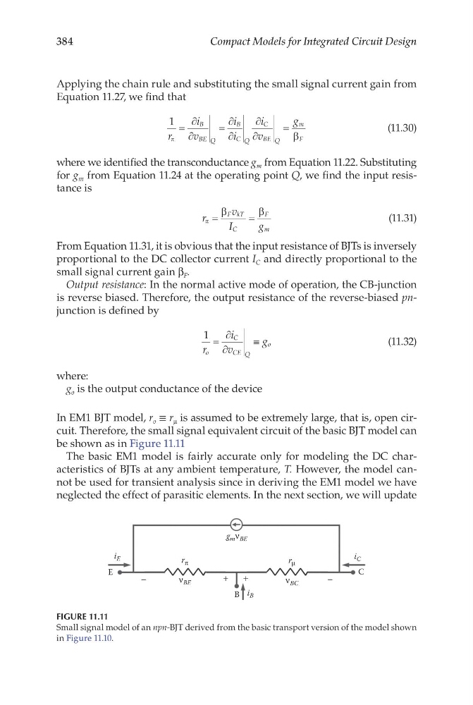
In EM1 BJT model, r o ≡ r μ is assumed to be extremely large, that is, open circuit. Therefore, the small signal equivalent circuit of the basic BJT model can
be shown as in Figure 11.11
The basic EM1 model is fairly accurate only for modeling the DC characteristics of BJTs at any ambient temperature, T. However, the model cannot be used for transient analysis since in deriving the EM1 model we have
neglected the effect of parasitic elements. In the next section, we will update
E
i E
r μ
B i B
C
i C
g m ν BE
r π
ν BC
ν BE
+
+
−
−
FIGURE 11.11
Small signal model of an npn-BJT derived from the basic transport version of the model shown
in Figure 11.10.
Compact Models for Integrated Circuit Design
Applying the chain rule and substituting the small signal current gain from
Equation 11.27, we find that
1
r
i
v
i
i
i
v
g
B
BE Q
B
C Q
C
BE Q
m
F
π
β
=
∂
∂
=
∂
∂
∂
∂
=
(11.30)
where we identified the transconductance g m from Equation 11.22. Substituting
for g m from Equation 11.24 at the operating point Q, we find the input resistance is
r
v
I
g
F kT
C
F
m
π
β
β
=
=
(11.31)
From Equation 11.31, it is obvious that the input resistance of BJTs is inversely
proportional to the DC collector current I C and directly proportional to the
small signal current gain β F .
Output resistance: In the normal active mode of operation, the CB-junction
is reverse biased. Therefore, the output resistance of the reverse-biased pnjunction is defined by
1
r
i
v
g
o
C
CE Q
o
=
∂
∂
≡
(11.32)
where:
g o is the output conductance of the device
In EM1 BJT model, r o ≡ r μ is assumed to be extremely large, that is, open circuit. Therefore, the small signal equivalent circuit of the basic BJT model can
be shown as in Figure 11.11
The basic EM1 model is fairly accurate only for modeling the DC characteristics of BJTs at any ambient temperature, T. However, the model cannot be used for transient analysis since in deriving the EM1 model we have
neglected the effect of parasitic elements. In the next section, we will update
E
i E
r μ
B i B
C
i C
g m ν BE
r π
ν BC
ν BE
+
+
−
−
FIGURE 11.11
Small signal model of an npn-BJT derived from the basic transport version of the model shown
in Figure 11.10.