

374
Compact Models for Integrated Circuit Design
voltage BV CB , and a decrease in the base-width modulation by the collector
voltage at a cost of collector terminal series resistance R C .
11.3 Basic Operation of BJTs
In order to describe the basic operation of BJTs, let us consider the structure
and biasing condition shown in Figure 11.3.
In a typical npn-BJT operation, an external potential, V BE (≈ 0.7 V), is applied
across the EB-junction to forward bias it, as shown in Figure 11.3. Electrons
are injected into the base by the emitter. (Also, holes are injected into the emitter
but their numbers are much lower because of the relative values of N a and N d .) If the
effective base width W B << L n (electron diffusion length) in the base, most of
the injected electrons get into the collector without recombining. A few do
recombine; the holes necessary for this are supplied as the base current, I B . The
electrons reaching the collector are collected across the CB-junction depletion
region (X dCB ) under the reverse bias CB-junction, V BC , and generates collector
current, I C . The carrier transport process is shown in Figure 11.4a and the
circuit representation of an npn-BJT is shown in Figure 11.4b. In Figure 11.4,
I E represents the emitter current. Conventionally, the current flowing into the
device terminal is defined as positive.
Since most of the injected electrons reach the collector, only a few holes are
injected into the emitter; therefore, I B << I C . As a result, the BJT device has a
substantial current gain (I C /I B ). Note that the built-in electric field across the base
also aids electron transport from E to C.
Base
Contact
Emitter
Collector
n+ buried layer
n-Epitaxial layer
n+ emitter
p+ isolation
p-base
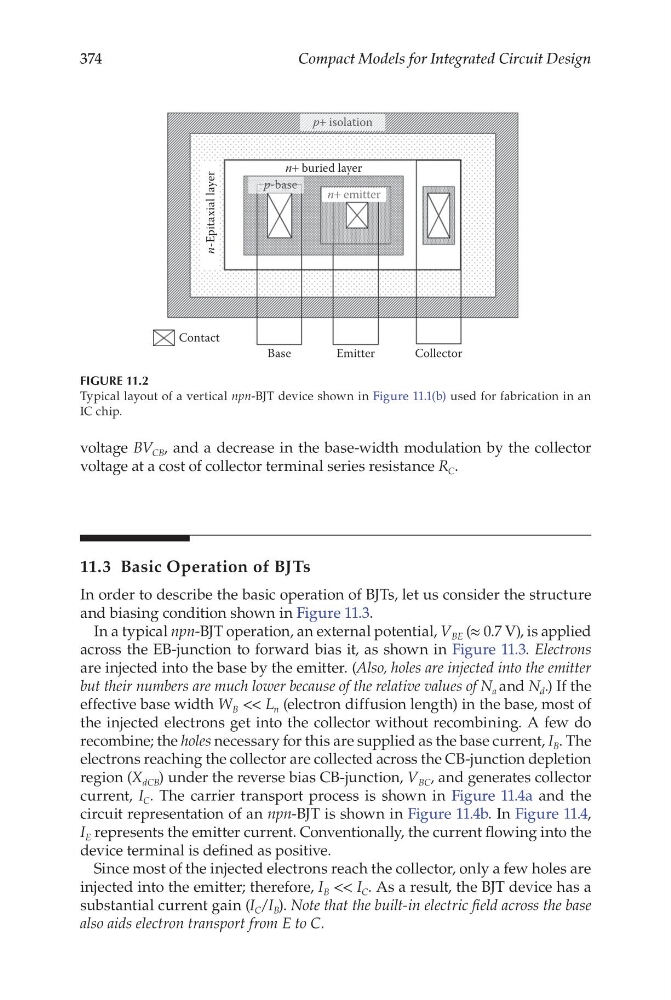
FIGURE 11.2
Typical layout of a vertical npn-BJT device shown in Figure 11.1(b) used for fabrication in an
IC chip.
Compact Models for Integrated Circuit Design
voltage BV CB , and a decrease in the base-width modulation by the collector
voltage at a cost of collector terminal series resistance R C .
11.3 Basic Operation of BJTs
In order to describe the basic operation of BJTs, let us consider the structure
and biasing condition shown in Figure 11.3.
In a typical npn-BJT operation, an external potential, V BE (≈ 0.7 V), is applied
across the EB-junction to forward bias it, as shown in Figure 11.3. Electrons
are injected into the base by the emitter. (Also, holes are injected into the emitter
but their numbers are much lower because of the relative values of N a and N d .) If the
effective base width W B << L n (electron diffusion length) in the base, most of
the injected electrons get into the collector without recombining. A few do
recombine; the holes necessary for this are supplied as the base current, I B . The
electrons reaching the collector are collected across the CB-junction depletion
region (X dCB ) under the reverse bias CB-junction, V BC , and generates collector
current, I C . The carrier transport process is shown in Figure 11.4a and the
circuit representation of an npn-BJT is shown in Figure 11.4b. In Figure 11.4,
I E represents the emitter current. Conventionally, the current flowing into the
device terminal is defined as positive.
Since most of the injected electrons reach the collector, only a few holes are
injected into the emitter; therefore, I B << I C . As a result, the BJT device has a
substantial current gain (I C /I B ). Note that the built-in electric field across the base
also aids electron transport from E to C.
Base
Contact
Emitter
Collector
n+ buried layer
n-Epitaxial layer
n+ emitter
p+ isolation
p-base
FIGURE 11.2
Typical layout of a vertical npn-BJT device shown in Figure 11.1(b) used for fabrication in an
IC chip.