

373
Bipolar Junction Transistor Compact Models
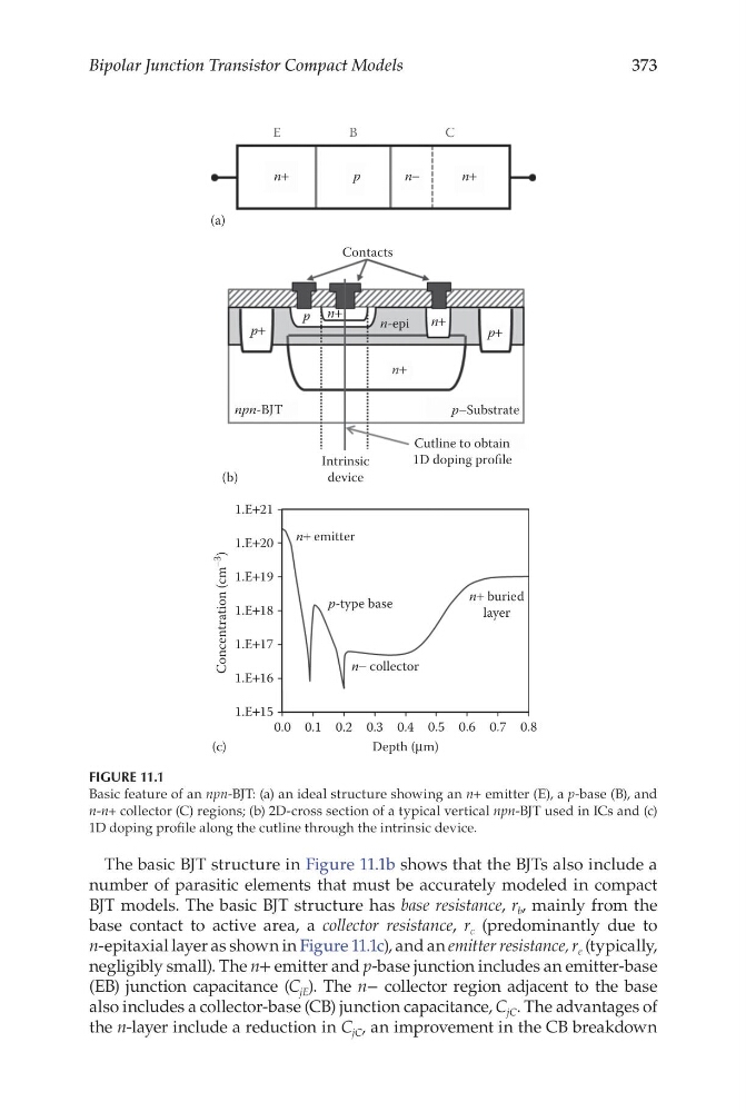
The basic BJT structure in Figure 11.1b shows that the BJTs also include a
number of parasitic elements that must be accurately modeled in compact
BJT models. The basic BJT structure has base resistance, r b , mainly from the
base contact to active area, a collector resistance, r c (predominantly due to
n- epitaxial layer as shown in Figure 11.1c), and an emitter resistance, r e (typically,
negligibly small). The n+ emitter and p-base junction includes an emitter-base
(EB) junction capacitance (C jE ). The n− collector region adjacent to the base
also includes a collector-base (CB) junction capacitance, C jC . The advantages of
the n-layer include a reduction in C jC , an improvement in the CB breakdown
(a)
E
n+
n+
p
n −
B
C
(b)
Intrinsic
device
Cutline to obtain
1D doping profile
n-epi
n+
n+
p+
n+
p+
npn-BJT
p–Substrate
p
Contacts
(c)
1.E+21
1.E+20
1.E+19
1.E+18
1.E+17
1.E+16
1.E+15
0.0 0.1 0.2 0.3 0.4
Depth (μm)
0.5 0.6 0.7 0.8
n+ emitter
n+ buried
layer
n− collector
p-type base
Concentration (cm
−3
)
FIGURE 11.1
Basic feature of an npn-BJT: (a) an ideal structure showing an n+ emitter (E), a p-base (B), and
n-n+ collector (C) regions; (b) 2D-cross section of a typical vertical npn-BJT used in ICs and (c)
1D doping profile along the cutline through the intrinsic device.
Bipolar Junction Transistor Compact Models
The basic BJT structure in Figure 11.1b shows that the BJTs also include a
number of parasitic elements that must be accurately modeled in compact
BJT models. The basic BJT structure has base resistance, r b , mainly from the
base contact to active area, a collector resistance, r c (predominantly due to
n- epitaxial layer as shown in Figure 11.1c), and an emitter resistance, r e (typically,
negligibly small). The n+ emitter and p-base junction includes an emitter-base
(EB) junction capacitance (C jE ). The n− collector region adjacent to the base
also includes a collector-base (CB) junction capacitance, C jC . The advantages of
the n-layer include a reduction in C jC , an improvement in the CB breakdown
(a)
E
n+
n+
p
n −
B
C
(b)
Intrinsic
device
Cutline to obtain
1D doping profile
n-epi
n+
n+
p+
n+
p+
npn-BJT
p–Substrate
p
Contacts
(c)
1.E+21
1.E+20
1.E+19
1.E+18
1.E+17
1.E+16
1.E+15
0.0 0.1 0.2 0.3 0.4
Depth (μm)
0.5 0.6 0.7 0.8
n+ emitter
n+ buried
layer
n− collector
p-type base
Concentration (cm
−3
)
FIGURE 11.1
Basic feature of an npn-BJT: (a) an ideal structure showing an n+ emitter (E), a p-base (B), and
n-n+ collector (C) regions; (b) 2D-cross section of a typical vertical npn-BJT used in ICs and (c)
1D doping profile along the cutline through the intrinsic device.