

366
Compact Models for Integrated Circuit Design
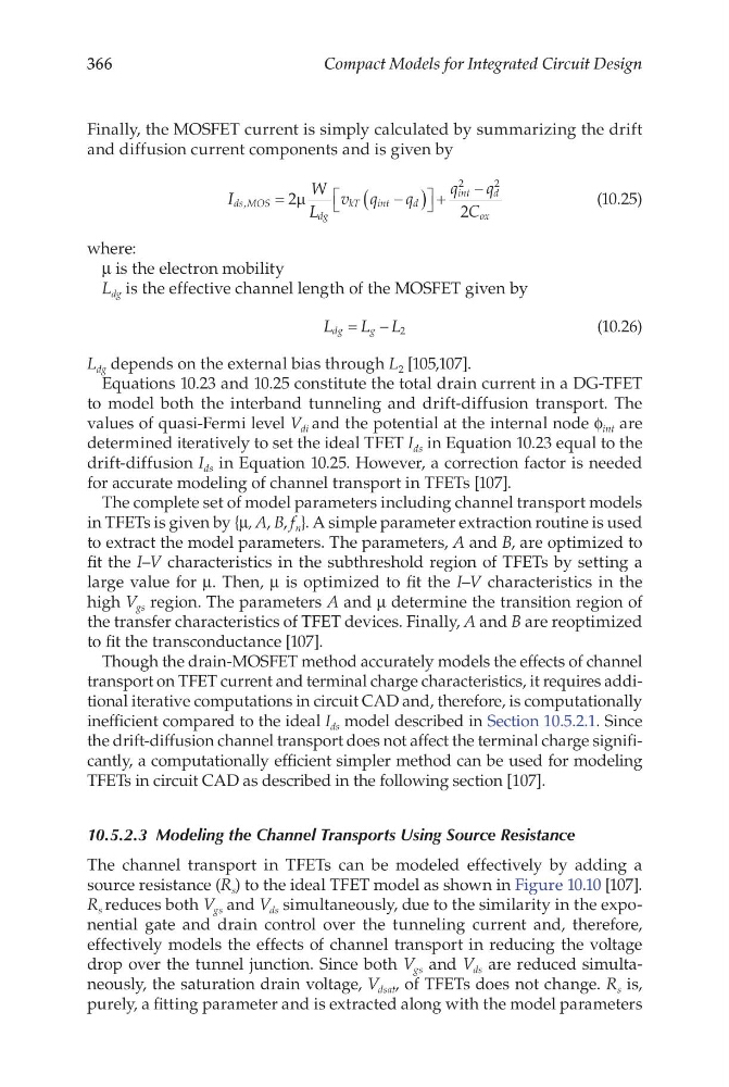
Finally, the MOSFET current is simply calculated by summarizing the drift
and diffusion current components and is given by
I
W
L
v q
q
q
q
C
ds MOS
dg
kT
int
d
int
d
ox
,
=
−
(
)
+
−
2
2
2
2
µ
(10.25)
where:
μ is the electron mobility
L dg is the effective channel length of the MOSFET given by
L
L L
dg
g
= − 2
(10.26)
L dg depends on the external bias through L 2 [105,107].
Equations 10.23 and 10.25 constitute the total drain current in a DG-TFET
to model both the interband tunneling and drift-diffusion transport. The
values of quasi-Fermi level V di and the potential at the internal node f int are
determined iteratively to set the ideal TFET I ds in Equation 10.23 equal to the
drift-diffusion I ds in Equation 10.25. However, a correction factor is needed
for accurate modeling of channel transport in TFETs [107].
The complete set of model parameters including channel transport models
in TFETs is given by {μ, A, B, f n }. A simple parameter extraction routine is used
to extract the model parameters. The parameters, A and B, are optimized to
fit the I–V characteristics in the subthreshold region of TFETs by setting a
large value for μ. Then, μ is optimized to fit the I–V characteristics in the
high V gs region. The parameters A and μ determine the transition region of
the transfer characteristics of TFET devices. Finally, A and B are reoptimized
to fit the transconductance [107].
Though the drain-MOSFET method accurately models the effects of channel
transport on TFET current and terminal charge characteristics, it requires additional iterative computations in circuit CAD and, therefore, is computationally
inefficient compared to the ideal I ds model described in Section 10.5.2.1. Since
the drift-diffusion channel transport does not affect the terminal charge significantly, a computationally efficient simpler method can be used for modeling
TFETs in circuit CAD as described in the following section [107].
10.5.2.3 Modeling the Channel Transports Using Source Resistance
The channel transport in TFETs can be modeled effectively by adding a
source resistance (R s ) to the ideal TFET model as shown in Figure 10.10 [107].
R s reduces both V gs and V ds simultaneously, due to the similarity in the exponential gate and drain control over the tunneling current and, therefore,
effectively models the effects of channel transport in reducing the voltage
drop over the tunnel junction. Since both V gs and V ds are reduced simultaneously, the saturation drain voltage, V dsat , of TFETs does not change. R s is,
purely, a fitting parameter and is extracted along with the model parameters
Compact Models for Integrated Circuit Design
Finally, the MOSFET current is simply calculated by summarizing the drift
and diffusion current components and is given by
I
W
L
v q
q
q
q
C
ds MOS
dg
kT
int
d
int
d
ox
,
=
−
(
)
+
−
2
2
2
2
µ
(10.25)
where:
μ is the electron mobility
L dg is the effective channel length of the MOSFET given by
L
L L
dg
g
= − 2
(10.26)
L dg depends on the external bias through L 2 [105,107].
Equations 10.23 and 10.25 constitute the total drain current in a DG-TFET
to model both the interband tunneling and drift-diffusion transport. The
values of quasi-Fermi level V di and the potential at the internal node f int are
determined iteratively to set the ideal TFET I ds in Equation 10.23 equal to the
drift-diffusion I ds in Equation 10.25. However, a correction factor is needed
for accurate modeling of channel transport in TFETs [107].
The complete set of model parameters including channel transport models
in TFETs is given by {μ, A, B, f n }. A simple parameter extraction routine is used
to extract the model parameters. The parameters, A and B, are optimized to
fit the I–V characteristics in the subthreshold region of TFETs by setting a
large value for μ. Then, μ is optimized to fit the I–V characteristics in the
high V gs region. The parameters A and μ determine the transition region of
the transfer characteristics of TFET devices. Finally, A and B are reoptimized
to fit the transconductance [107].
Though the drain-MOSFET method accurately models the effects of channel
transport on TFET current and terminal charge characteristics, it requires additional iterative computations in circuit CAD and, therefore, is computationally
inefficient compared to the ideal I ds model described in Section 10.5.2.1. Since
the drift-diffusion channel transport does not affect the terminal charge significantly, a computationally efficient simpler method can be used for modeling
TFETs in circuit CAD as described in the following section [107].
10.5.2.3 Modeling the Channel Transports Using Source Resistance
The channel transport in TFETs can be modeled effectively by adding a
source resistance (R s ) to the ideal TFET model as shown in Figure 10.10 [107].
R s reduces both V gs and V ds simultaneously, due to the similarity in the exponential gate and drain control over the tunneling current and, therefore,
effectively models the effects of channel transport in reducing the voltage
drop over the tunnel junction. Since both V gs and V ds are reduced simultaneously, the saturation drain voltage, V dsat , of TFETs does not change. R s is,
purely, a fitting parameter and is extracted along with the model parameters