

365
Beyond-CMOS Transistor Models: Tunnel FETs
and drift-diffusion currents at the same value. From the discussion in the
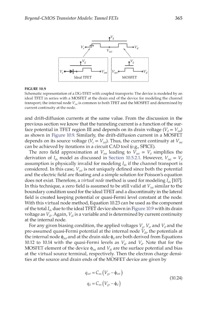
previous section we know that the tunneling current is a function of the surface potential in TFET region III and depends on its drain voltage (V d = V int )
as shown in Figure 10.9. Similarly, the drift-diffusion current in a MOSFET
depends on its source voltage (V s = V int ). Thus, the current continuity at V int
can be achieved by iterations in a circuit CAD tool (e.g., SPICE).
The zero field approximation at V int leading to V int = V d simplifies the
derivation of I ds model as discussed in Section 10.5.2.1. However, V int = V d
assumption is physically invalid for modeling I ds if the channel transport is
considered. In this case, V int is not uniquely defined since both the potential
and the electric field are floating and a simple solution for Poisson’s equation
does not exist. Therefore, a virtual node method is used for modeling I ds [107].
In this technique, a zero field is assumed to be still valid at V int similar to the
boundary condition used for the ideal TFET and a discontinuity in the lateral
field is created keeping potential or quasi-Fermi level constant at the node.
With this virtual node method, Equation 10.23 can be used as the component
of the total I ds due to the ideal TFET device shown in Figure 10.9 with its drain
voltage as V di . Again, V di is a variable and is determined by current continuity
at the internal node.
For any given biasing condition, the applied voltages V g , V s , and V d and the
pre-assumed quasi-Fermi potential at the internal node V di , the potentials at
the internal node f int and at the drain side f d are both derived from Equations
10.12 to 10.14 with the quasi-Fermi levels as V di and V d . Note that for the
MOSFET element of the device f int and V di are the surface potential and bias
at the virtual source terminal, respectively. Then the electron charge densities at the source and drain ends of the MOSFET device are given by
q
C V
q C V
int
o x
g s
i nt
d
o x
g s
d
=
−
(
)
=
−
(
)
φ
φ
(10.24)
Ideal TFET
MOSFET
V g
V s
V int V int
V d
V g
V d
V int
V s
V g
FIGURE 10.9
Schematic representation of a DG-TFET with coupled transports: The device is modeled by an
ideal TFET in series with a MOSFET at the drain end of the device for modeling the channel
transport; the internal node V int is common to both TFET and the MOSFET and determined by
current continuity at the node.
Beyond-CMOS Transistor Models: Tunnel FETs
and drift-diffusion currents at the same value. From the discussion in the
previous section we know that the tunneling current is a function of the surface potential in TFET region III and depends on its drain voltage (V d = V int )
as shown in Figure 10.9. Similarly, the drift-diffusion current in a MOSFET
depends on its source voltage (V s = V int ). Thus, the current continuity at V int
can be achieved by iterations in a circuit CAD tool (e.g., SPICE).
The zero field approximation at V int leading to V int = V d simplifies the
derivation of I ds model as discussed in Section 10.5.2.1. However, V int = V d
assumption is physically invalid for modeling I ds if the channel transport is
considered. In this case, V int is not uniquely defined since both the potential
and the electric field are floating and a simple solution for Poisson’s equation
does not exist. Therefore, a virtual node method is used for modeling I ds [107].
In this technique, a zero field is assumed to be still valid at V int similar to the
boundary condition used for the ideal TFET and a discontinuity in the lateral
field is created keeping potential or quasi-Fermi level constant at the node.
With this virtual node method, Equation 10.23 can be used as the component
of the total I ds due to the ideal TFET device shown in Figure 10.9 with its drain
voltage as V di . Again, V di is a variable and is determined by current continuity
at the internal node.
For any given biasing condition, the applied voltages V g , V s , and V d and the
pre-assumed quasi-Fermi potential at the internal node V di , the potentials at
the internal node f int and at the drain side f d are both derived from Equations
10.12 to 10.14 with the quasi-Fermi levels as V di and V d . Note that for the
MOSFET element of the device f int and V di are the surface potential and bias
at the virtual source terminal, respectively. Then the electron charge densities at the source and drain ends of the MOSFET device are given by
q
C V
q C V
int
o x
g s
i nt
d
o x
g s
d
=
−
(
)
=
−
(
)
φ
φ
(10.24)
Ideal TFET
MOSFET
V g
V s
V int V int
V d
V g
V d
V int
V s
V g
FIGURE 10.9
Schematic representation of a DG-TFET with coupled transports: The device is modeled by an
ideal TFET in series with a MOSFET at the drain end of the device for modeling the channel
transport; the internal node V int is common to both TFET and the MOSFET and determined by
current continuity at the node.