

364
Compact Models for Integrated Circuit Design
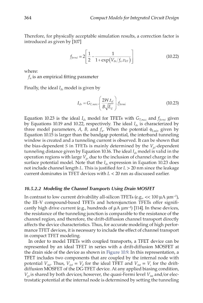
Therefore, for physically acceptable simulation results, a correction factor is
introduced as given by [107]
f
V f v
fermi
ds n kT
=
− +
(
)
2
1
2
1
1 exp
.
(10.22)
where:
f n is an empirical fitting parameter
Finally, the ideal I ds model is given by
I
G
W t
B E
f
ds
T, max
si
g
fermi
=
.
. .
2
(10.23)
Equation 10.23 is the ideal I ds model for TFETs with G T,max and f fermi given
by Equations 10.19 and 10.22, respectively. The ideal I ds is characterized by
three model parameters, A, B, and f n . When the potential f I,min given by
Equation 10.15 is larger than the bandgap potential, the interband tunneling
window is created and a tunneling current is observed. It can be shown that
the bias-dependent S in TFETs is mainly determined by the V gs -dependent
tunneling distance given by Equation 10.16. The ideal I ds model is valid in the
operation regions with large V gs due to the inclusion of channel charge in the
surface potential model. Note that the I ds expression in Equation 10.23 does
not include channel length L. This is justified for L > 20 nm since the leakage
current dominates in TFET devices with L < 20 nm as discussed earlier.
10.5.2.2 Modeling the Channel Transports Using Drain MOSFET
In contrast to low current drivability all-silicon TFETs (e.g., << 100 μA μm −1 ),
the III–V compound-based TFETs and heterojunction TFETs offer significantly high drive current (e.g., hundreds of μA μm −1 ) [114]. In these devices,
the resistance of the tunneling junction is comparable to the resistance of the
channel region, and therefore, the drift-diffusion channel transport directly
affects the device characteristics. Thus, for accurate modeling of high performance TFET devices, it is necessary to include the effect of channel transport
in compact TFET modeling.
In order to model TFETs with coupled transports, a TFET device can be
represented by an ideal TFET in series with a drift-diffusion MOSFET at
the drain side of the device as shown in Figure 10.9. In this representation, a
TFET includes two components that are coupled by the internal node with
potential V int . Thus, V int = V d for the ideal TFET and V int = V s for the driftdiffusion MOSFET of the DG-TFET device. At any applied biasing condition,
V gs is shared by both devices; however, the quasi-Fermi level V int and/or electrostatic potential at the internal node is determined by setting the tunneling
Compact Models for Integrated Circuit Design
Therefore, for physically acceptable simulation results, a correction factor is
introduced as given by [107]
f
V f v
fermi
ds n kT
=
− +
(
)
2
1
2
1
1 exp
.
(10.22)
where:
f n is an empirical fitting parameter
Finally, the ideal I ds model is given by
I
G
W t
B E
f
ds
T, max
si
g
fermi
=
.
. .
2
(10.23)
Equation 10.23 is the ideal I ds model for TFETs with G T,max and f fermi given
by Equations 10.19 and 10.22, respectively. The ideal I ds is characterized by
three model parameters, A, B, and f n . When the potential f I,min given by
Equation 10.15 is larger than the bandgap potential, the interband tunneling
window is created and a tunneling current is observed. It can be shown that
the bias-dependent S in TFETs is mainly determined by the V gs -dependent
tunneling distance given by Equation 10.16. The ideal I ds model is valid in the
operation regions with large V gs due to the inclusion of channel charge in the
surface potential model. Note that the I ds expression in Equation 10.23 does
not include channel length L. This is justified for L > 20 nm since the leakage
current dominates in TFET devices with L < 20 nm as discussed earlier.
10.5.2.2 Modeling the Channel Transports Using Drain MOSFET
In contrast to low current drivability all-silicon TFETs (e.g., << 100 μA μm −1 ),
the III–V compound-based TFETs and heterojunction TFETs offer significantly high drive current (e.g., hundreds of μA μm −1 ) [114]. In these devices,
the resistance of the tunneling junction is comparable to the resistance of the
channel region, and therefore, the drift-diffusion channel transport directly
affects the device characteristics. Thus, for accurate modeling of high performance TFET devices, it is necessary to include the effect of channel transport
in compact TFET modeling.
In order to model TFETs with coupled transports, a TFET device can be
represented by an ideal TFET in series with a drift-diffusion MOSFET at
the drain side of the device as shown in Figure 10.9. In this representation, a
TFET includes two components that are coupled by the internal node with
potential V int . Thus, V int = V d for the ideal TFET and V int = V s for the driftdiffusion MOSFET of the DG-TFET device. At any applied biasing condition,
V gs is shared by both devices; however, the quasi-Fermi level V int and/or electrostatic potential at the internal node is determined by setting the tunneling