

363
Beyond-CMOS Transistor Models: Tunnel FETs
where:
f dg = u s v kT is the surface potential of the channel region (III) DG-MOSFET
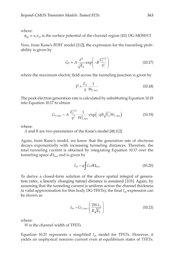
Now, from Kane’s BTBT model [112], the expression for the tunneling probability is given by
G
A
F
E
B
E
F
T
g
g
=
−
2
3 2
exp
/
(10.17)
where the maximum electric field across the tunneling junction is given by
F
E
q W
g
T, min
=
1
(10.18)
The peak electron generation rate is calculated by substituting Equation 10.18
into Equation 10.17 to obtain
G
A
E
q W
qB E W
T max
g
T min
g
T min
,
/
,
,
.
e xp
=
−
(
)
3 2
2
2
1
(10.19)
where:
A and B are two parameters of the Kane’s model [48,112]
Again, from Kane’s model, we know that the generation rate of electrons
decays exponentially with increasing tunneling distances. Therefore, the
total tunneling current is obtained by integrating Equation 10.17 over the
tunneling space dΩ tun and is given by
I
q G d
ds
T
t un
=
∫
Ω
(10.20)
To derive a closed-form solution of the above spatial integral of generation rates, a linearly changing tunnel distance is assumed [103]. Again, by
assuming that the tunneling current is uniform across the channel thickness
(a valid approximation for thin body DG-TFETs), the final I ds expression can
be shown as
I
G
W t
B E
ds
T max
si
g
=
,
.
.
2
(10.21)
where:
W is the channel width of TFETs
Equation 10.21 represents a simplified I ds model for TFETs. However, it
yields an unphysical nonzero current even at equilibrium states of TFETs.
Beyond-CMOS Transistor Models: Tunnel FETs
where:
f dg = u s v kT is the surface potential of the channel region (III) DG-MOSFET
Now, from Kane’s BTBT model [112], the expression for the tunneling probability is given by
G
A
F
E
B
E
F
T
g
g
=
−
2
3 2
exp
/
(10.17)
where the maximum electric field across the tunneling junction is given by
F
E
q W
g
T, min
=
1
(10.18)
The peak electron generation rate is calculated by substituting Equation 10.18
into Equation 10.17 to obtain
G
A
E
q W
qB E W
T max
g
T min
g
T min
,
/
,
,
.
e xp
=
−
(
)
3 2
2
2
1
(10.19)
where:
A and B are two parameters of the Kane’s model [48,112]
Again, from Kane’s model, we know that the generation rate of electrons
decays exponentially with increasing tunneling distances. Therefore, the
total tunneling current is obtained by integrating Equation 10.17 over the
tunneling space dΩ tun and is given by
I
q G d
ds
T
t un
=
∫
Ω
(10.20)
To derive a closed-form solution of the above spatial integral of generation rates, a linearly changing tunnel distance is assumed [103]. Again, by
assuming that the tunneling current is uniform across the channel thickness
(a valid approximation for thin body DG-TFETs), the final I ds expression can
be shown as
I
G
W t
B E
ds
T max
si
g
=
,
.
.
2
(10.21)
where:
W is the channel width of TFETs
Equation 10.21 represents a simplified I ds model for TFETs. However, it
yields an unphysical nonzero current even at equilibrium states of TFETs.