

362
Compact Models for Integrated Circuit Design
du
dx
q n
kT
F u v y E
kT
F
E
kT
x
i
si
ch
g
u
u
g
s
=
=
−
−
(
)
−
(
)
0
2
3 2
1 2
2
2
2
3
2
0
ε
/
/
( )
/
/
(10.13)
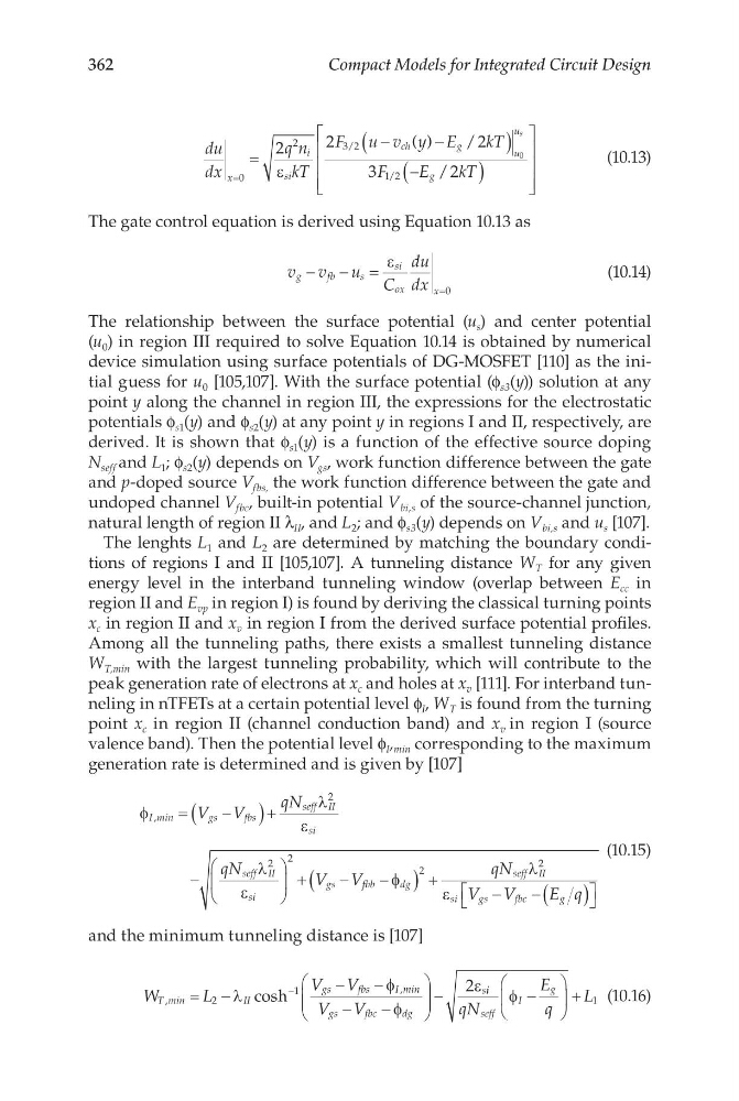
The gate control equation is derived using Equation 10.13 as
v v u C
du
dx
g
f b
s
si
ox
x
− − =
=
ε
0
(10.14)
The relationship between the surface potential (u s ) and center potential
(u 0 ) in region III required to solve Equation 10.14 is obtained by numerical
device simulation using surface potentials of DG-MOSFET [110] as the initial guess for u 0 [105,107]. With the surface potential (f s3 (y)) solution at any
point y along the channel in region III, the expressions for the electrostatic
potentials f s1 (y) and f s2 (y) at any point y in regions I and II, respectively, are
derived. It is shown that f s1 (y) is a function of the effective source doping
N seff and L 1 ; f s2 (y) depends on V gs , work function difference between the gate
and p-doped source V fbs, the work function difference between the gate and
undoped channel V fbc , built-in potential V bi,s of the source-channel junction,
natural length of region II λ II , and L 2 ; and f s3 (y) depends on V bi,s and u s [107].
The lenghts L 1 and L 2 are determined by matching the boundary conditions of regions I and II [105,107]. A tunneling distance W T for any given
energy level in the interband tunneling window (overlap between E cc in
region II and E vp in region I) is found by deriving the classical turning points
x c in region II and x v in region I from the derived surface potential profiles.
Among all the tunneling paths, there exists a smallest tunneling distance
W T,min with the largest tunneling probability, which will contribute to the
peak generation rate of electrons at x c and holes at x v [111]. For interband tunneling in nTFETs at a certain potential level f I , W T is found from the turning
point x c in region II (channel conduction band) and x v in region I (source
valence band). Then the potential level f I , min corresponding to the maximum
generation rate is determined and is given by [107]
φ
λ
ε
λ
ε
I min
gs
fbs
seff II
si
seff II
si
gs
V V
qN
qN
V V
,
=
−
(
) +
−
+
−
2
2 2
f fbb
d g
seff II
si
gs
fbc
g
qN
V V
E q
−
(
) +
−
− ( )
φ
λ
ε
2
2
(10.15)
and the minimum tunneling distance is [107]
W
L
V V
V V
T min
II
gs
fbs
Imin
gs
fbc
d g
s
,
,
cosh
= −
−
−
−
−
−
−
2
1
2
λ
φ
φ
ε i i
seff
I
g
qN
E
q
L
φ −
+ 1 (10.16)
Compact Models for Integrated Circuit Design
du
dx
q n
kT
F u v y E
kT
F
E
kT
x
i
si
ch
g
u
u
g
s
=
=
−
−
(
)
−
(
)
0
2
3 2
1 2
2
2
2
3
2
0
ε
/
/
( )
/
/
(10.13)
The gate control equation is derived using Equation 10.13 as
v v u C
du
dx
g
f b
s
si
ox
x
− − =
=
ε
0
(10.14)
The relationship between the surface potential (u s ) and center potential
(u 0 ) in region III required to solve Equation 10.14 is obtained by numerical
device simulation using surface potentials of DG-MOSFET [110] as the initial guess for u 0 [105,107]. With the surface potential (f s3 (y)) solution at any
point y along the channel in region III, the expressions for the electrostatic
potentials f s1 (y) and f s2 (y) at any point y in regions I and II, respectively, are
derived. It is shown that f s1 (y) is a function of the effective source doping
N seff and L 1 ; f s2 (y) depends on V gs , work function difference between the gate
and p-doped source V fbs, the work function difference between the gate and
undoped channel V fbc , built-in potential V bi,s of the source-channel junction,
natural length of region II λ II , and L 2 ; and f s3 (y) depends on V bi,s and u s [107].
The lenghts L 1 and L 2 are determined by matching the boundary conditions of regions I and II [105,107]. A tunneling distance W T for any given
energy level in the interband tunneling window (overlap between E cc in
region II and E vp in region I) is found by deriving the classical turning points
x c in region II and x v in region I from the derived surface potential profiles.
Among all the tunneling paths, there exists a smallest tunneling distance
W T,min with the largest tunneling probability, which will contribute to the
peak generation rate of electrons at x c and holes at x v [111]. For interband tunneling in nTFETs at a certain potential level f I , W T is found from the turning
point x c in region II (channel conduction band) and x v in region I (source
valence band). Then the potential level f I , min corresponding to the maximum
generation rate is determined and is given by [107]
φ
λ
ε
λ
ε
I min
gs
fbs
seff II
si
seff II
si
gs
V V
qN
qN
V V
,
=
−
(
) +
−
+
−
2
2 2
f fbb
d g
seff II
si
gs
fbc
g
qN
V V
E q
−
(
) +
−
− ( )
φ
λ
ε
2
2
(10.15)
and the minimum tunneling distance is [107]
W
L
V V
V V
T min
II
gs
fbs
Imin
gs
fbc
d g
s
,
,
cosh
= −
−
−
−
−
−
−
2
1
2
λ
φ
φ
ε i i
seff
I
g
qN
E
q
L
φ −
+ 1 (10.16)