

361
Beyond-CMOS Transistor Models: Tunnel FETs
10.5.2.1 Ideal Drain Current Model
In the present state-of-the-art silicon TFETs with low-drive current, the channel
transport is insignificant due to the comparatively large tunnel-junction resistance. Thus, for the simplicity of modeling TFETs, the channel transport can be
neglected to develop an ideal TFET model by zero field approximation along the
channel [105,107].
Let us consider a DG-nTFET shown in Figure 10.8a to illustrate the compact
modeling techniques in TFETs. In order to derive I ds model for DG-TFETs,
the entire device is divided into three regions as shown in Figure 10.8a:
the source junction region (I), channel junction region (II), and the channel transport region (III) [105,107]. With the zero field approximation, the
quasi-Fermi potential at the boundary of regions II and III is equal to V ds ,
and therefore, the channel transports can be neglected to develop an ideal I ds
model. Though a gradient of the electrostatic potential exists in region III, the
quasi-Fermi potential at the internal node V int is smaller than V ds . In principle,
V int can be determined by ensuring current continuity between the quantum
tunneling current and the drift-diffusion current.
In order to develop an ideal I ds model without the channel transport, electrostatic potentials in TFETs are solved to derive the expression for tunneling
current. The charges in region III are considered to model the exponential
dependence of the output characteristics and the terminal capacitance properties of TFETs [105,107]. The potential solutions together with the zero electric
field approximation in region III form the boundary conditions for region II.
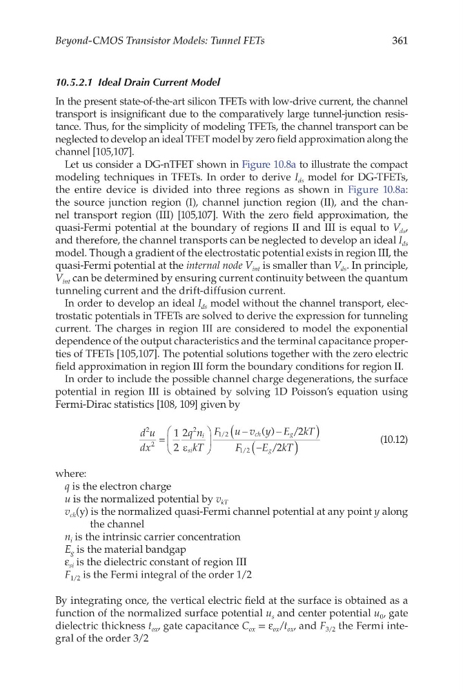
In order to include the possible channel charge degenerations, the surface
potential in region III is obtained by solving 1D Poisson’s equation using
Fermi-Dirac statistics [108, 109] given by
d u
dx
q n
kT
F u v y E kT
F
E kT
i
si
ch
g
g
2
2
2
1 2
1 2
1
2
2
2
2
=
−
−
(
)
−
(
ε
/
/
( )
/
/
) )
(10.12)
where:
q is the electron charge
u is the normalized potential by v kT
v ch (y) is the normalized quasi-Fermi channel potential at any point y along
the channel
n i is the intrinsic carrier concentration
E g is the material bandgap
ε si is the dielectric constant of region III
F 1/2 is the Fermi integral of the order 1/2
By integrating once, the vertical electric field at the surface is obtained as a
function of the normalized surface potential u s and center potential u 0 , gate
dielectric thickness t ox , gate capacitance C ox = ε ox /t ox , and F 3/2 the Fermi integral of the order 3/2
Beyond-CMOS Transistor Models: Tunnel FETs
10.5.2.1 Ideal Drain Current Model
In the present state-of-the-art silicon TFETs with low-drive current, the channel
transport is insignificant due to the comparatively large tunnel-junction resistance. Thus, for the simplicity of modeling TFETs, the channel transport can be
neglected to develop an ideal TFET model by zero field approximation along the
channel [105,107].
Let us consider a DG-nTFET shown in Figure 10.8a to illustrate the compact
modeling techniques in TFETs. In order to derive I ds model for DG-TFETs,
the entire device is divided into three regions as shown in Figure 10.8a:
the source junction region (I), channel junction region (II), and the channel transport region (III) [105,107]. With the zero field approximation, the
quasi-Fermi potential at the boundary of regions II and III is equal to V ds ,
and therefore, the channel transports can be neglected to develop an ideal I ds
model. Though a gradient of the electrostatic potential exists in region III, the
quasi-Fermi potential at the internal node V int is smaller than V ds . In principle,
V int can be determined by ensuring current continuity between the quantum
tunneling current and the drift-diffusion current.
In order to develop an ideal I ds model without the channel transport, electrostatic potentials in TFETs are solved to derive the expression for tunneling
current. The charges in region III are considered to model the exponential
dependence of the output characteristics and the terminal capacitance properties of TFETs [105,107]. The potential solutions together with the zero electric
field approximation in region III form the boundary conditions for region II.
In order to include the possible channel charge degenerations, the surface
potential in region III is obtained by solving 1D Poisson’s equation using
Fermi-Dirac statistics [108, 109] given by
d u
dx
q n
kT
F u v y E kT
F
E kT
i
si
ch
g
g
2
2
2
1 2
1 2
1
2
2
2
2
=
−
−
(
)
−
(
ε
/
/
( )
/
/
) )
(10.12)
where:
q is the electron charge
u is the normalized potential by v kT
v ch (y) is the normalized quasi-Fermi channel potential at any point y along
the channel
n i is the intrinsic carrier concentration
E g is the material bandgap
ε si is the dielectric constant of region III
F 1/2 is the Fermi integral of the order 1/2
By integrating once, the vertical electric field at the surface is obtained as a
function of the normalized surface potential u s and center potential u 0 , gate
dielectric thickness t ox , gate capacitance C ox = ε ox /t ox , and F 3/2 the Fermi integral of the order 3/2