

352
Compact Models for Integrated Circuit Design
distribution function f s (E) of the source electrons is shown in Figure 10.4a,
whereas Figure 10.4b shows the expanded f s (E) versus E distribution. Since the
electrons with E > kT of f s (E) are effectively filtered out from tunneling as shown
in Figure 10.4, the current transport in TFETs is a sub-kT process. Thus, it can be
considered that the electronic system is effectively cooled down acting as a conventional MOSFET at a lower temperature. Thus, in a TFET, primarily the cold
carriers participate in the transport process, resulting in a subthreshold slope of
less than 60 mV per decade. Note that in MOSFETs the subthreshold conduction is limited by Boltzmann distribution with higher-kT process (Chapters 4
and 5), thus limiting S to 60 mV per decade of current at room temperature.
The interband tunneling process in a TFET shown in Figure 10.4 is similar
to a band-pass filter action wherein the high energy carriers are filtered out.
This filtering function enables to achieve an S of below 60 mV per decade of
current for TFETs. However, the channel conduction band E cc can be pulled
up or down by a small change in V gs , that is, the tunneling width can be
effectively changed by V gs [38,49]. As a result, the value of S in a TFET is not a
constant and depends on V gs increasing with the increasing V gs .
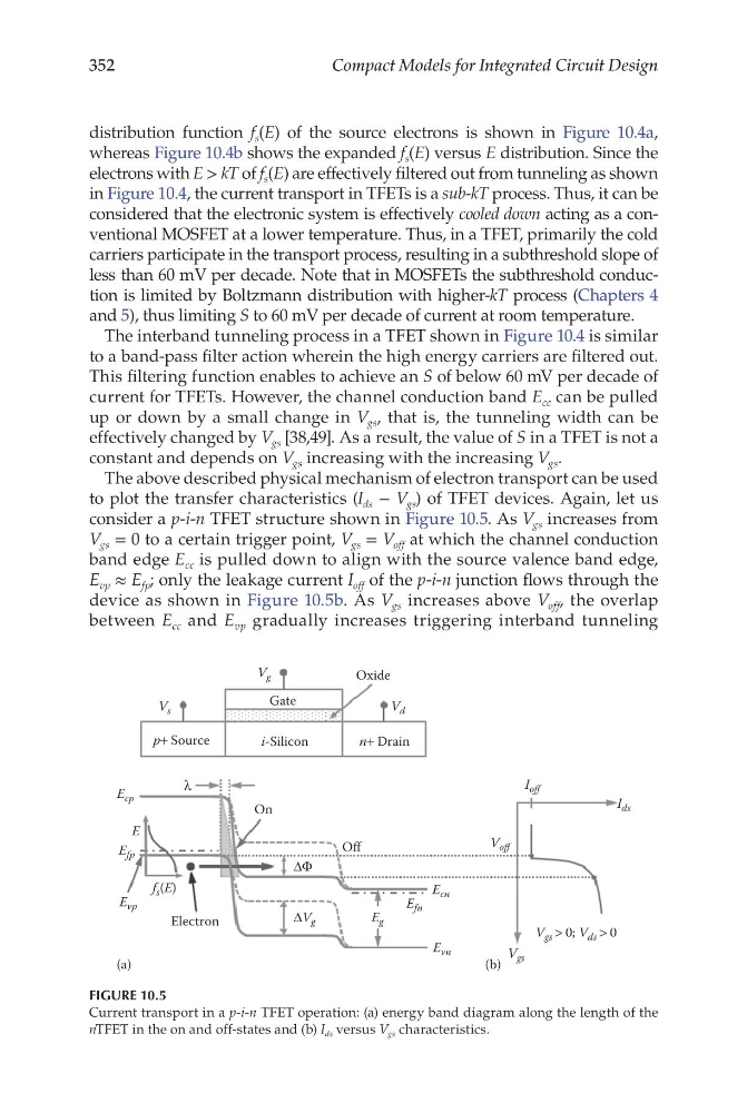
The above described physical mechanism of electron transport can be used
to plot the transfer characteristics (I ds − V gs ) of TFET devices. Again, let us
consider a p-i-n TFET structure shown in Figure 10.5. As V gs increases from
V gs = 0 to a certain trigger point, V gs = V off at which the channel conduction
band edge E cc is pulled down to align with the source valence band edge,
E vp ≈ E fp ; only the leakage current I off of the p-i-n junction flows through the
device as shown in Figure 10.5b. As V gs increases above V off , the overlap
between E cc and E vp gradually increases triggering interband tunneling
V s
λ
E cp
V off
V gs
V gs > 0; V ds > 0
E cn
E fn
E g
E vn
ΔV g
ΔΦ
I off
I ds
Electron
(a)
(b)
On
Off
E
E fp
E vp
f s (E)
V g
Oxide
Gate
p+ Source
n+ Drain
i-Silicon
V d
FIGURE 10.5
Current transport in a p-i-n TFET operation: (a) energy band diagram along the length of the
nTFET in the on and off-states and (b) I ds versus V gs characteristics.
Compact Models for Integrated Circuit Design
distribution function f s (E) of the source electrons is shown in Figure 10.4a,
whereas Figure 10.4b shows the expanded f s (E) versus E distribution. Since the
electrons with E > kT of f s (E) are effectively filtered out from tunneling as shown
in Figure 10.4, the current transport in TFETs is a sub-kT process. Thus, it can be
considered that the electronic system is effectively cooled down acting as a conventional MOSFET at a lower temperature. Thus, in a TFET, primarily the cold
carriers participate in the transport process, resulting in a subthreshold slope of
less than 60 mV per decade. Note that in MOSFETs the subthreshold conduction is limited by Boltzmann distribution with higher-kT process (Chapters 4
and 5), thus limiting S to 60 mV per decade of current at room temperature.
The interband tunneling process in a TFET shown in Figure 10.4 is similar
to a band-pass filter action wherein the high energy carriers are filtered out.
This filtering function enables to achieve an S of below 60 mV per decade of
current for TFETs. However, the channel conduction band E cc can be pulled
up or down by a small change in V gs , that is, the tunneling width can be
effectively changed by V gs [38,49]. As a result, the value of S in a TFET is not a
constant and depends on V gs increasing with the increasing V gs .
The above described physical mechanism of electron transport can be used
to plot the transfer characteristics (I ds − V gs ) of TFET devices. Again, let us
consider a p-i-n TFET structure shown in Figure 10.5. As V gs increases from
V gs = 0 to a certain trigger point, V gs = V off at which the channel conduction
band edge E cc is pulled down to align with the source valence band edge,
E vp ≈ E fp ; only the leakage current I off of the p-i-n junction flows through the
device as shown in Figure 10.5b. As V gs increases above V off , the overlap
between E cc and E vp gradually increases triggering interband tunneling
V s
λ
E cp
V off
V gs
V gs > 0; V ds > 0
E cn
E fn
E g
E vn
ΔV g
ΔΦ
I off
I ds
Electron
(a)
(b)
On
Off
E
E fp
E vp
f s (E)
V g
Oxide
Gate
p+ Source
n+ Drain
i-Silicon
V d
FIGURE 10.5
Current transport in a p-i-n TFET operation: (a) energy band diagram along the length of the
nTFET in the on and off-states and (b) I ds versus V gs characteristics.