

353
Beyond-CMOS Transistor Models: Tunnel FETs
and the drain current I ds increases. Since the Fermi tail of f s (E) is cut off from
the tunneling window, only the electrons with E < kT contribute to current
transport, resulting in a sharp increase in I ds with steep slope as shown in
Figure 10.5b. On further increase of V gs to the target supply voltage, the tunneling window reaches the corresponding final width ΔΦ and the sub-kT
electrons tunnel from the source to the channel. The tunneled electrons are
then transported to the drain by supply voltage, V ds , generating a steady flow
of I ds in the device as shown in Figure 10.5b.
In TFETs, I off is low due to the filtering of electrons from the high energy
Fermi tail. The value can be further reduced by widening the tunneling barrier at drain junction [4,16,57].
10.3.4 Subthreshold Swing
In Chapter 4, we have shown that S for a MOSFET device is defined by
S d
I dV
ds
gs
= (
)
−
log
1 in units of mV per (decade I ds ). For the TFETs, the tunnel
current can be described approximately by [48]
I
aV F
b
F
ds
eff
≅
−
exp
(10.5)
where:
a and b are the coefficients that depend on the material properties of the
tunnel junction and the cross-sectional area of the device
V eff and F are the effective reverse bias and electric field at the tunnel junction, respectively
The coefficients a and b are given by [16,38]
a
Aq
m
E
b
m E
q
r
g
r g
=
= −
3
2 2
3
2
8
4 2
3
*
*
π
(10.6)
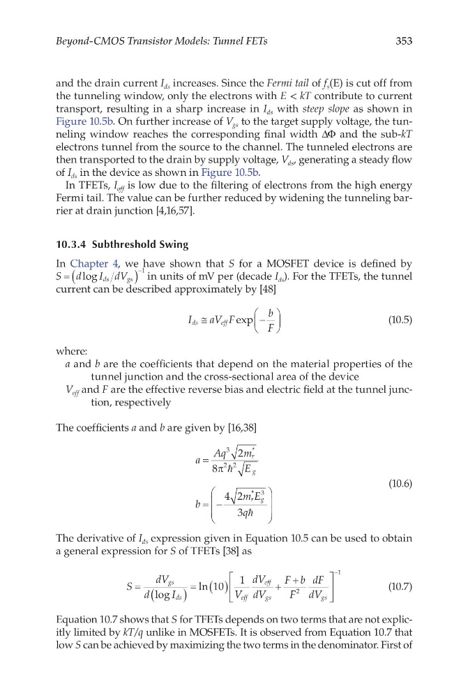
The derivative of I ds expression given in Equation 10.5 can be used to obtain
a general expression for S of TFETs [38] as
S
dV
d
I
V
dV
dV
F b
F
dF
dV
gs
ds
eff
eff
gs
gs
=
(
)
= ( )
+
+
−
log
ln 10
1
2
1
(10.7)
Equation 10.7 shows that S for TFETs depends on two terms that are not explicitly limited by kT/q unlike in MOSFETs. It is observed from Equation 10.7 that
low S can be achieved by maximizing the two terms in the denominator. First of
Beyond-CMOS Transistor Models: Tunnel FETs
and the drain current I ds increases. Since the Fermi tail of f s (E) is cut off from
the tunneling window, only the electrons with E < kT contribute to current
transport, resulting in a sharp increase in I ds with steep slope as shown in
Figure 10.5b. On further increase of V gs to the target supply voltage, the tunneling window reaches the corresponding final width ΔΦ and the sub-kT
electrons tunnel from the source to the channel. The tunneled electrons are
then transported to the drain by supply voltage, V ds , generating a steady flow
of I ds in the device as shown in Figure 10.5b.
In TFETs, I off is low due to the filtering of electrons from the high energy
Fermi tail. The value can be further reduced by widening the tunneling barrier at drain junction [4,16,57].
10.3.4 Subthreshold Swing
In Chapter 4, we have shown that S for a MOSFET device is defined by
S d
I dV
ds
gs
= (
)
−
log
1 in units of mV per (decade I ds ). For the TFETs, the tunnel
current can be described approximately by [48]
I
aV F
b
F
ds
eff
≅
−
exp
(10.5)
where:
a and b are the coefficients that depend on the material properties of the
tunnel junction and the cross-sectional area of the device
V eff and F are the effective reverse bias and electric field at the tunnel junction, respectively
The coefficients a and b are given by [16,38]
a
Aq
m
E
b
m E
q
r
g
r g
=
= −
3
2 2
3
2
8
4 2
3
*
*
π
(10.6)
The derivative of I ds expression given in Equation 10.5 can be used to obtain
a general expression for S of TFETs [38] as
S
dV
d
I
V
dV
dV
F b
F
dF
dV
gs
ds
eff
eff
gs
gs
=
(
)
= ( )
+
+
−
log
ln 10
1
2
1
(10.7)
Equation 10.7 shows that S for TFETs depends on two terms that are not explicitly limited by kT/q unlike in MOSFETs. It is observed from Equation 10.7 that
low S can be achieved by maximizing the two terms in the denominator. First of