

351
Beyond-CMOS Transistor Models: Tunnel FETs
proportional to (ΔΦ + E g )/λ) along the channel. Higher F can be achieved by
different ways: (1) thinner t ox or higher dielectric constant (high-k) gate oxide;
(2) low E g channel materials such as silicon germanium (SiGe) or Ge [54,55]
or a thin layer of SiGe material between the source and the channel [56]; and
(3) light-m r * materials for source-channel junction. Low E g channel materials
increase I off of TFETs and, therefore, require device optimization.
10.3.3 Device Characteristics
Let us consider a p-i-n structure for an nTFET device operation as shown in
Figure 10.3. Figure 10.3a shows the off-state of the device with zero bias and
on-state with V gs > 0 and V ds > 0. In the TFET off-state (broken line curve in
Figure 10.3a), the conduction band edge of the channel is located above the
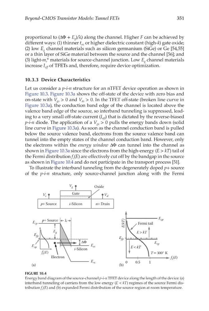
valence band edge of the source, so interband tunneling is suppressed, leading to a very small off-state current (I off ) that is dictated by the reverse-biased
p-i-n diode. The application of a V gs > 0 pulls the energy bands down (solid
line curve in Figure 10.3a). As soon as the channel conduction band is pulled
below the source valence band, electrons from the source valence band can
tunnel into the empty states of the channel conduction band. However, only
the electrons within the energy window ΔΦ can tunnel into the channel as
shown in Figure 10.3a since the electrons from the high-energy (E > kT) tail of
the Fermi distribution f s (E) are effectively cut off by the bandgap in the source
as shown in Figure 10.4 and do not participate in the transport process [51].
To illustrate the interband tunneling from the degenerately doped p+ source
of the p-i-n structure, only source-channel junction along with the Fermi
(a)
(b)
0
0.5
T = 300° K
1
f s (E)
E fp
E(kT)
E cp
E vp
E < kT
E > kT
V s
E cp
E fp
E g
λ
ΔΦ
E vp
Electron
i-Silicon
f s (E)
E cc
E vc
V g
V d
Oxide
Gate
p+ Source
p+ Source
n+ Drain
i-Silicon
Fermi tail
FIGURE 10.4
Energy band diagram of the source-channel p-i-n TFET device along the length of the device: (a)
interband tunneling of carriers from the low energy (E < kT) regimes of the source Fermi distribution f s (E) and (b) expanded Fermi distribution of the source region at room temperature.
Beyond-CMOS Transistor Models: Tunnel FETs
proportional to (ΔΦ + E g )/λ) along the channel. Higher F can be achieved by
different ways: (1) thinner t ox or higher dielectric constant (high-k) gate oxide;
(2) low E g channel materials such as silicon germanium (SiGe) or Ge [54,55]
or a thin layer of SiGe material between the source and the channel [56]; and
(3) light-m r * materials for source-channel junction. Low E g channel materials
increase I off of TFETs and, therefore, require device optimization.
10.3.3 Device Characteristics
Let us consider a p-i-n structure for an nTFET device operation as shown in
Figure 10.3. Figure 10.3a shows the off-state of the device with zero bias and
on-state with V gs > 0 and V ds > 0. In the TFET off-state (broken line curve in
Figure 10.3a), the conduction band edge of the channel is located above the
valence band edge of the source, so interband tunneling is suppressed, leading to a very small off-state current (I off ) that is dictated by the reverse-biased
p-i-n diode. The application of a V gs > 0 pulls the energy bands down (solid
line curve in Figure 10.3a). As soon as the channel conduction band is pulled
below the source valence band, electrons from the source valence band can
tunnel into the empty states of the channel conduction band. However, only
the electrons within the energy window ΔΦ can tunnel into the channel as
shown in Figure 10.3a since the electrons from the high-energy (E > kT) tail of
the Fermi distribution f s (E) are effectively cut off by the bandgap in the source
as shown in Figure 10.4 and do not participate in the transport process [51].
To illustrate the interband tunneling from the degenerately doped p+ source
of the p-i-n structure, only source-channel junction along with the Fermi
(a)
(b)
0
0.5
T = 300° K
1
f s (E)
E fp
E(kT)
E cp
E vp
E < kT
E > kT
V s
E cp
E fp
E g
λ
ΔΦ
E vp
Electron
i-Silicon
f s (E)
E cc
E vc
V g
V d
Oxide
Gate
p+ Source
p+ Source
n+ Drain
i-Silicon
Fermi tail
FIGURE 10.4
Energy band diagram of the source-channel p-i-n TFET device along the length of the device: (a)
interband tunneling of carriers from the low energy (E < kT) regimes of the source Fermi distribution f s (E) and (b) expanded Fermi distribution of the source region at room temperature.