

349
Beyond-CMOS Transistor Models: Tunnel FETs
to the slope of the energy bands, so that qF = (ΔΦ + E g )/λ. Therefore, the
tunneling probability for TFETs is given by [51]
T E
m E
E
g
g
( ) exp
*
≅
−
+
(
)
4 2
3
3
λ
∆Φ
(10.2)
where:
ΔΦ is the energy range over which the tunneling can take place
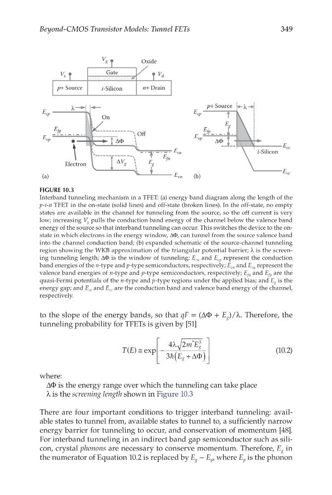
λ is the screening length shown in Figure 10.3
There are four important conditions to trigger interband tunneling: available states to tunnel from, available states to tunnel to, a sufficiently narrow
energy barrier for tunneling to occur, and conservation of momentum [48].
For interband tunneling in an indirect band gap semiconductor such as silicon, crystal phonons are necessary to conserve momentum. Therefore, E g in
the numerator of Equation 10.2 is replaced by E g − E p , where E p is the phonon
(a)
(b)
λ
ΔΦ
E vp
E fp
E g
E cc
E vc
E cp
p+ Source
i-Silicon
V s
E cp
λ
E fp
E vp
Electron
On
Off
ΔΦ
ΔV g
E cn
E fn
E vn
E g
V g
V d
Oxide
Gate
p+ Source
n+ Drain
i-Silicon
FIGURE 10.3
Interband tunneling mechanism in a TFET: (a) energy band diagram along the length of the
p-i-n TFET in the on-state (solid lines) and off-state (broken lines). In the off-state, no empty
states are available in the channel for tunneling from the source, so the off current is very
low; increasing V g pulls the conduction band energy of the channel below the valence band
energy of the source so that interband tunneling can occur. This switches the device to the onstate in which electrons in the energy window, ΔΦ, can tunnel from the source valence band
into the channel conduction band; (b) expanded schematic of the source-channel tunneling
region showing the WKB approximation of the triangular potential barrier; λ is the screening tunneling length; ΔΦ is the window of tunneling; E cn and E cp represent the conduction
band energies of the n-type and p-type semiconductors, respectively; E vn and E vp represent the
valence band energies of n-type and p-type semiconductors, respectively; E fn and E fp are the
quasi-Fermi potentials of the n-type and p-type regions under the applied bias; and E g is the
energy gap; and E cc and E vc are the conduction band and valence band energy of the channel,
respectively.
Beyond-CMOS Transistor Models: Tunnel FETs
to the slope of the energy bands, so that qF = (ΔΦ + E g )/λ. Therefore, the
tunneling probability for TFETs is given by [51]
T E
m E
E
g
g
( ) exp
*
≅
−
+
(
)
4 2
3
3
λ
∆Φ
(10.2)
where:
ΔΦ is the energy range over which the tunneling can take place
λ is the screening length shown in Figure 10.3
There are four important conditions to trigger interband tunneling: available states to tunnel from, available states to tunnel to, a sufficiently narrow
energy barrier for tunneling to occur, and conservation of momentum [48].
For interband tunneling in an indirect band gap semiconductor such as silicon, crystal phonons are necessary to conserve momentum. Therefore, E g in
the numerator of Equation 10.2 is replaced by E g − E p , where E p is the phonon
(a)
(b)
λ
ΔΦ
E vp
E fp
E g
E cc
E vc
E cp
p+ Source
i-Silicon
V s
E cp
λ
E fp
E vp
Electron
On
Off
ΔΦ
ΔV g
E cn
E fn
E vn
E g
V g
V d
Oxide
Gate
p+ Source
n+ Drain
i-Silicon
FIGURE 10.3
Interband tunneling mechanism in a TFET: (a) energy band diagram along the length of the
p-i-n TFET in the on-state (solid lines) and off-state (broken lines). In the off-state, no empty
states are available in the channel for tunneling from the source, so the off current is very
low; increasing V g pulls the conduction band energy of the channel below the valence band
energy of the source so that interband tunneling can occur. This switches the device to the onstate in which electrons in the energy window, ΔΦ, can tunnel from the source valence band
into the channel conduction band; (b) expanded schematic of the source-channel tunneling
region showing the WKB approximation of the triangular potential barrier; λ is the screening tunneling length; ΔΦ is the window of tunneling; E cn and E cp represent the conduction
band energies of the n-type and p-type semiconductors, respectively; E vn and E vp represent the
valence band energies of n-type and p-type semiconductors, respectively; E fn and E fp are the
quasi-Fermi potentials of the n-type and p-type regions under the applied bias; and E g is the
energy gap; and E cc and E vc are the conduction band and valence band energy of the channel,
respectively.