

348
Compact Models for Integrated Circuit Design
10.3.2 Tunneling Mechanism
In a TFET the primary injection mechanism of charge carriers is interband
tunneling [21] in which the charge carriers transfer from one energy band
into another at a heavily doped p+n+ junction in contrast to MOSFETs where
the charge carriers are thermally injected over a barrier. Interband tunneling was first observed in 1957 by Esaki [21] while studying narrow forwardbiased p–n junctions called tunnel diode. However, the interband tunneling
concept was first used by Zener in 1934 to explain the dielectric breakdown
at a high electric field [17] and is known as the Zener tunneling, which is also
referred to as the band-to-band tunneling (BTBT).
The Zener or interband tunneling can be realized in a reverse-biased p-i-n
structure as shown in Figure 10.2. In a TFET, the interband tunneling can be
switched on and off abruptly by controlling the band bending in the channel
region by applying V gs . As shown in Figure 10.2a, for a p-i-n TFET structure
at V gs = 0, the tunneling barrier is large, and the device is in the off-state.
A V gs > 0 pulls the energy bands down and reduces the tunneling barrier.
Due to reduced energy barrier, the carriers can tunnel from the valence band
in the source to the conduction band in the channel and the tunneling current
increases. For a p+n+ tunnel junction, the tunneling current is determined by
integrating the product of charge flux and the tunneling probability T(E) from
the energy states on the p+ side to those on the n+ side. And, T(E) is calculated by applying Wentzel–Kramers–Brillouin (WKB) approximation of the
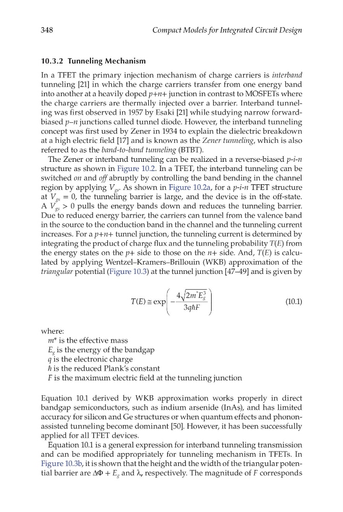
triangular potential (Figure 10.3) at the tunnel junction [47–49] and is given by
T E
m E
q F
g
( ) exp
*
≅
−
4 2
3
3
(10.1)
where:
m* is the effective mass
E g is the energy of the bandgap
q is the electronic charge
is the reduced Plank’s constant
F is the maximum electric field at the tunneling junction
Equation 10.1 derived by WKB approximation works properly in direct
bandgap semiconductors, such as indium arsenide (InAs), and has limited
accuracy for silicon and Ge structures or when quantum effects and phononassisted tunneling become dominant [50]. However, it has been successfully
applied for all TFET devices.
Equation 10.1 is a general expression for interband tunneling transmission
and can be modified appropriately for tunneling mechanism in TFETs. In
Figure 10.3b, it is shown that the height and the width of the triangular potential barrier are ΔΦ + E g and λ, respectively. The magnitude of F corresponds
Compact Models for Integrated Circuit Design
10.3.2 Tunneling Mechanism
In a TFET the primary injection mechanism of charge carriers is interband
tunneling [21] in which the charge carriers transfer from one energy band
into another at a heavily doped p+n+ junction in contrast to MOSFETs where
the charge carriers are thermally injected over a barrier. Interband tunneling was first observed in 1957 by Esaki [21] while studying narrow forwardbiased p–n junctions called tunnel diode. However, the interband tunneling
concept was first used by Zener in 1934 to explain the dielectric breakdown
at a high electric field [17] and is known as the Zener tunneling, which is also
referred to as the band-to-band tunneling (BTBT).
The Zener or interband tunneling can be realized in a reverse-biased p-i-n
structure as shown in Figure 10.2. In a TFET, the interband tunneling can be
switched on and off abruptly by controlling the band bending in the channel
region by applying V gs . As shown in Figure 10.2a, for a p-i-n TFET structure
at V gs = 0, the tunneling barrier is large, and the device is in the off-state.
A V gs > 0 pulls the energy bands down and reduces the tunneling barrier.
Due to reduced energy barrier, the carriers can tunnel from the valence band
in the source to the conduction band in the channel and the tunneling current
increases. For a p+n+ tunnel junction, the tunneling current is determined by
integrating the product of charge flux and the tunneling probability T(E) from
the energy states on the p+ side to those on the n+ side. And, T(E) is calculated by applying Wentzel–Kramers–Brillouin (WKB) approximation of the
triangular potential (Figure 10.3) at the tunnel junction [47–49] and is given by
T E
m E
q F
g
( ) exp
*
≅
−
4 2
3
3
(10.1)
where:
m* is the effective mass
E g is the energy of the bandgap
q is the electronic charge
is the reduced Plank’s constant
F is the maximum electric field at the tunneling junction
Equation 10.1 derived by WKB approximation works properly in direct
bandgap semiconductors, such as indium arsenide (InAs), and has limited
accuracy for silicon and Ge structures or when quantum effects and phononassisted tunneling become dominant [50]. However, it has been successfully
applied for all TFET devices.
Equation 10.1 is a general expression for interband tunneling transmission
and can be modified appropriately for tunneling mechanism in TFETs. In
Figure 10.3b, it is shown that the height and the width of the triangular potential barrier are ΔΦ + E g and λ, respectively. The magnitude of F corresponds