

347
Beyond-CMOS Transistor Models: Tunnel FETs
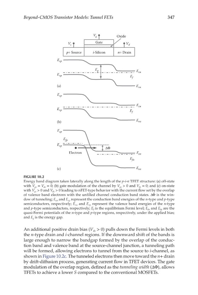
An additional positive drain bias (V ds > 0) pulls down the Fermi levels in both
the n-type drain and i-channel regions. If the downward shift of the bands is
large enough to narrow the bandgap formed by the overlap of the conduction band and valence band at the source-channel junction, a tunneling path
will be formed, allowing electrons to tunnel from the source to i-channel, as
shown in Figure 10.2c. The tunneled electrons then move toward the n+ drain
by drift-diffusion process, generating current flow in TFET devices. The gate
modulation of the overlap region, defined as the tunneling width (ΔΦ), allows
TFETs to achieve a lower S compared to the conventional MOSFETs.
E cp
V s
V g
V d
Oxide
Gate
(a)
(b)
(c)
n+ Drain
p+ Source
i-Silicon
E g
E f
E cn
E vn
E cn
E f
E vn
E cn
E fn
E vn
E vp
E cp
E vp
E cp
E vp
Electron
ΔΦ
E fp
FIGURE 10.2
Energy band diagram taken laterally along the length of the p-i-n TFET structure: (a) off-state
with V gs = V ds = 0; (b) gate modulation of the channel by V gs > 0 and V ds = 0; and (c) on-state
with V gs > 0 and V ds > 0 leading to nFET-type behavior with the current flow set by the overlap
of valence band electrons with the unfilled channel conduction band states. ΔΦ is the window of tunneling; E cn and E cp represent the conduction band energies of the n-type and p-type
semiconductors, respectively; E vn and E vp represent the valence band energies of the n-type
and p-type semiconductors, respectively; E f is the equilibrium Fermi level; E fn and E fp are the
quasi-Fermi potentials of the n-type and p-type regions, respectively, under the applied bias;
and E g is the energy gap.
Beyond-CMOS Transistor Models: Tunnel FETs
An additional positive drain bias (V ds > 0) pulls down the Fermi levels in both
the n-type drain and i-channel regions. If the downward shift of the bands is
large enough to narrow the bandgap formed by the overlap of the conduction band and valence band at the source-channel junction, a tunneling path
will be formed, allowing electrons to tunnel from the source to i-channel, as
shown in Figure 10.2c. The tunneled electrons then move toward the n+ drain
by drift-diffusion process, generating current flow in TFET devices. The gate
modulation of the overlap region, defined as the tunneling width (ΔΦ), allows
TFETs to achieve a lower S compared to the conventional MOSFETs.
E cp
V s
V g
V d
Oxide
Gate
(a)
(b)
(c)
n+ Drain
p+ Source
i-Silicon
E g
E f
E cn
E vn
E cn
E f
E vn
E cn
E fn
E vn
E vp
E cp
E vp
E cp
E vp
Electron
ΔΦ
E fp
FIGURE 10.2
Energy band diagram taken laterally along the length of the p-i-n TFET structure: (a) off-state
with V gs = V ds = 0; (b) gate modulation of the channel by V gs > 0 and V ds = 0; and (c) on-state
with V gs > 0 and V ds > 0 leading to nFET-type behavior with the current flow set by the overlap
of valence band electrons with the unfilled channel conduction band states. ΔΦ is the window of tunneling; E cn and E cp represent the conduction band energies of the n-type and p-type
semiconductors, respectively; E vn and E vp represent the valence band energies of the n-type
and p-type semiconductors, respectively; E f is the equilibrium Fermi level; E fn and E fp are the
quasi-Fermi potentials of the n-type and p-type regions, respectively, under the applied bias;
and E g is the energy gap.