

338
Compact Models for Integrated Circuit Design
The expressions for terminal charges are continuous and are valid over subthreshold, linear, and saturation regimes of operation.
Equation 9.71 forms the C–V model for BSIM-CMG. The terminal charges
are used as state variables in the circuit simulation. All the capacitances are
derived from the terminal charges to ensure charge conservation. The capacitances are defined as
C
Q
V
ij
i
j
=
∂
∂
(9.72)
where:
i and j denote the multigate FET terminals
Note that C ij satisfies
C
C
ij
i
ij
j
∑ ∑
=
=0
(9.73)
due to charge conservation.
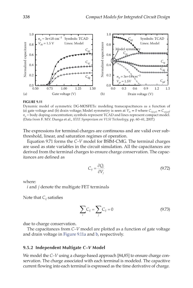
The capacitances from C–V model are plotted as a function of gate voltage
and drain voltage in Figure 9.11a and b, respectively.
9.5.2 Independent Multigate C–V Model
We model the C–V using a charge-based approach [84,85] to ensure charge conservation. The charge associated with each terminal is modeled. The capacitive
current flowing into each terminal is expressed as the time derivative of charge.
0.50
(a)
(b)
0.0
0.2
0.4
0.6
Normalized capacitance
0.8
1.0
0.0
0.2
0.4
0.6
Normalized capacitance
0.8
1.0
0.75
1.00
Gate voltage (V)
C dg
C sg
C gg
C sg
C dg
C gd
C gg
Model symmetry
C gs
Symbols: TCAD
n a = 3e+18 cm −3
V ds = 1.5 V
n a = 3e+18 cm
−3
V gs = 1.5V
Lines: Model
Symbols: TCAD
Lines: Model
1.25
1.50
0.0
0.6
Drain voltage (V)
0.3
0.9
1.2
1.5
FIGURE 9.11
Dynamic model of symmetric DG-MOSFETs: modeling transcapacitances as a function of
(a) gate voltage and (b) drain voltage; Model symmetry is seen at V ds = 0 where C dg(gd) = C sg(gs) ;
n a = body doping concentration; symbols represent TCAD and lines represent compact model.
(Data from F. M.V. Dunga et al., IEEE Symposium on VLSI Technology, pp. 60–61, 2007.)
Compact Models for Integrated Circuit Design
The expressions for terminal charges are continuous and are valid over subthreshold, linear, and saturation regimes of operation.
Equation 9.71 forms the C–V model for BSIM-CMG. The terminal charges
are used as state variables in the circuit simulation. All the capacitances are
derived from the terminal charges to ensure charge conservation. The capacitances are defined as
C
Q
V
ij
i
j
=
∂
∂
(9.72)
where:
i and j denote the multigate FET terminals
Note that C ij satisfies
C
C
ij
i
ij
j
∑ ∑
=
=0
(9.73)
due to charge conservation.
The capacitances from C–V model are plotted as a function of gate voltage
and drain voltage in Figure 9.11a and b, respectively.
9.5.2 Independent Multigate C–V Model
We model the C–V using a charge-based approach [84,85] to ensure charge conservation. The charge associated with each terminal is modeled. The capacitive
current flowing into each terminal is expressed as the time derivative of charge.
0.50
(a)
(b)
0.0
0.2
0.4
0.6
Normalized capacitance
0.8
1.0
0.0
0.2
0.4
0.6
Normalized capacitance
0.8
1.0
0.75
1.00
Gate voltage (V)
C dg
C sg
C gg
C sg
C dg
C gd
C gg
Model symmetry
C gs
Symbols: TCAD
n a = 3e+18 cm −3
V ds = 1.5 V
n a = 3e+18 cm
−3
V gs = 1.5V
Lines: Model
Symbols: TCAD
Lines: Model
1.25
1.50
0.0
0.6
Drain voltage (V)
0.3
0.9
1.2
1.5
FIGURE 9.11
Dynamic model of symmetric DG-MOSFETs: modeling transcapacitances as a function of
(a) gate voltage and (b) drain voltage; Model symmetry is seen at V ds = 0 where C dg(gd) = C sg(gs) ;
n a = body doping concentration; symbols represent TCAD and lines represent compact model.
(Data from F. M.V. Dunga et al., IEEE Symposium on VLSI Technology, pp. 60–61, 2007.)