

328
Compact Models for Integrated Circuit Design
A unique behavior of lightly doped DG-FETs with thin body is that the
inversion charge is no longer confined to interface and the entire film is
inverted. For any gate voltage, the electrostatic potential increases at the interfaces as well as in the volume of the film in all mode of device operation: the
depletion, weak inversion, and the strong inversion. As a result, the potential
shift or total band bending exceeds 2f B in every region and in the entire film.
This is referred to as the volume inversion [61, 63–65]. Due to volume inversion
(1) the potential as well as the inversion carrier density is nearly independent of
the position inside the body because of the negligible potential drop between
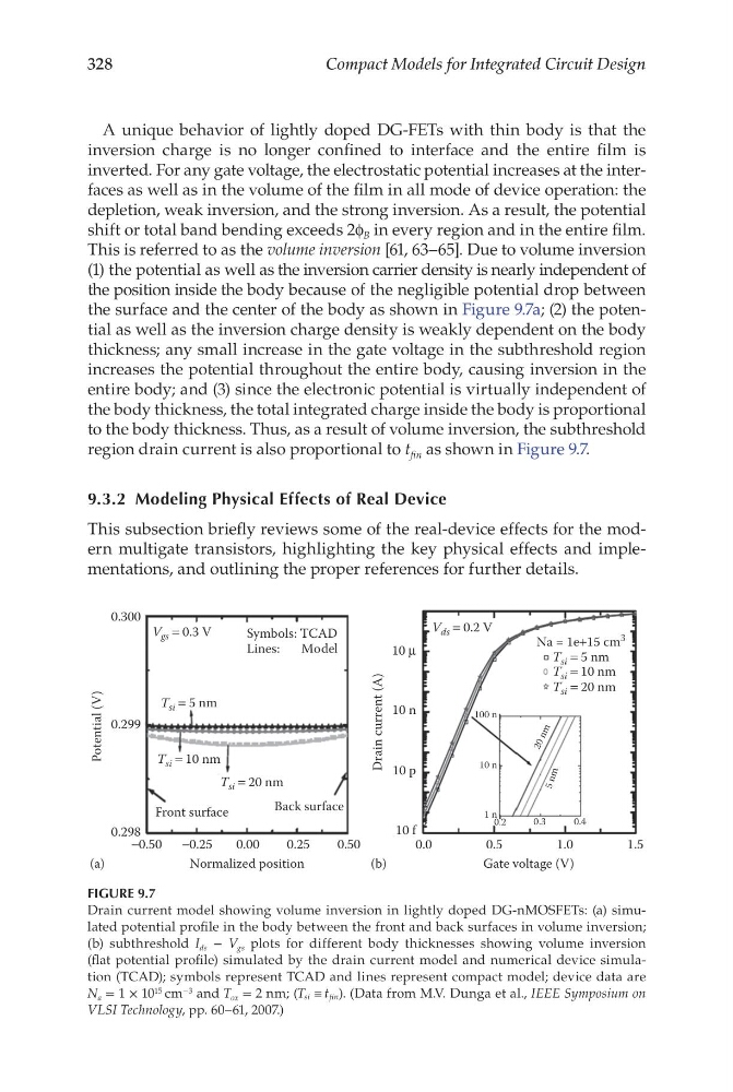
the surface and the center of the body as shown in Figure 9.7a; (2) the potential as well as the inversion charge density is weakly dependent on the body
thickness; any small increase in the gate voltage in the subthreshold region
increases the potential throughout the entire body, causing inversion in the
entire body; and (3) since the electronic potential is virtually independent of
the body thickness, the total integrated charge inside the body is proportional
to the body thickness. Thus, as a result of volume inversion, the subthreshold
region drain current is also proportional to t fin as shown in Figure 9.7.
9.3.2 Modeling Physical Effects of Real Device
This subsection briefly reviews some of the real-device effects for the modern multigate transistors, highlighting the key physical effects and implementations, and outlining the proper references for further details.
Drain current (A)
Gate voltage (V)
0.2
1 n
10 n
100 n
0.3
5 n m
2 0 n m
0.4
0.0
10 f
10 p
10 n
10 μ
V ds = 0.2 V
0.5
1.0
1.5
Na = 1e+15 cm
3
T si = 5 nm
T si = 10 nm
T si = 20 nm
Front surface
−0.50
0.298
0.299
Potential (V)
0.300
−0.25
0.00
Normalized position
0.25
0.50
Back surface
T si = 20 nm
T si = 10 nm
T si = 5 nm
Symbols: TCAD
Lines:
Model
V gs = 0.3 V
(a)
(b)
FIGURE 9.7
Drain current model showing volume inversion in lightly doped DG-nMOSFETs: (a) simulated potential profile in the body between the front and back surfaces in volume inversion;
(b) subthreshold I ds − V gs plots for different body thicknesses showing volume inversion
(flat potential profile) simulated by the drain current model and numerical device simulation (TCAD); symbols represent TCAD and lines represent compact model; device data are
N a = 1 × 10 15 cm −3 and T ox = 2 nm; (T t
si
fin
≡ ). (Data from M.V. Dunga et al., IEEE Symposium on
VLSI Technology, pp. 60–61, 2007.)
Compact Models for Integrated Circuit Design
A unique behavior of lightly doped DG-FETs with thin body is that the
inversion charge is no longer confined to interface and the entire film is
inverted. For any gate voltage, the electrostatic potential increases at the interfaces as well as in the volume of the film in all mode of device operation: the
depletion, weak inversion, and the strong inversion. As a result, the potential
shift or total band bending exceeds 2f B in every region and in the entire film.
This is referred to as the volume inversion [61, 63–65]. Due to volume inversion
(1) the potential as well as the inversion carrier density is nearly independent of
the position inside the body because of the negligible potential drop between
the surface and the center of the body as shown in Figure 9.7a; (2) the potential as well as the inversion charge density is weakly dependent on the body
thickness; any small increase in the gate voltage in the subthreshold region
increases the potential throughout the entire body, causing inversion in the
entire body; and (3) since the electronic potential is virtually independent of
the body thickness, the total integrated charge inside the body is proportional
to the body thickness. Thus, as a result of volume inversion, the subthreshold
region drain current is also proportional to t fin as shown in Figure 9.7.
9.3.2 Modeling Physical Effects of Real Device
This subsection briefly reviews some of the real-device effects for the modern multigate transistors, highlighting the key physical effects and implementations, and outlining the proper references for further details.
Drain current (A)
Gate voltage (V)
0.2
1 n
10 n
100 n
0.3
5 n m
2 0 n m
0.4
0.0
10 f
10 p
10 n
10 μ
V ds = 0.2 V
0.5
1.0
1.5
Na = 1e+15 cm
3
T si = 5 nm
T si = 10 nm
T si = 20 nm
Front surface
−0.50
0.298
0.299
Potential (V)
0.300
−0.25
0.00
Normalized position
0.25
0.50
Back surface
T si = 20 nm
T si = 10 nm
T si = 5 nm
Symbols: TCAD
Lines:
Model
V gs = 0.3 V
(a)
(b)
FIGURE 9.7
Drain current model showing volume inversion in lightly doped DG-nMOSFETs: (a) simulated potential profile in the body between the front and back surfaces in volume inversion;
(b) subthreshold I ds − V gs plots for different body thicknesses showing volume inversion
(flat potential profile) simulated by the drain current model and numerical device simulation (TCAD); symbols represent TCAD and lines represent compact model; device data are
N a = 1 × 10 15 cm −3 and T ox = 2 nm; (T t
si
fin
≡ ). (Data from M.V. Dunga et al., IEEE Symposium on
VLSI Technology, pp. 60–61, 2007.)