

327
Compact Models for Ultrathin Body FETs
where:
Q 0 = 2Q b + 5C si v kT , with C si = K si ε 0 /t fin
Q b is the fixed depletion charge and is given by qN b t fin
It is reported that the unified charge density model agrees very well with the
inversion charge density calculated using an exact equation for a wide range
of body doping concentration [60]. Then from Equation 9.44, the gradient in
V ch (y), term dV ch /dQ i can be calculated as a function of Q i using a simple but
accurate implicit equation for Q i [60]
dV
dy
d
dy
v
dQ
dy
Q
C v
Q
Q
C v
Q
ch
s
kT
i
b
si kT
i
b
si kT
i
=
+
+
+
+
−
φ
2
5
2
5
2
(9.45)
Equation 9.34 can be integrated analytically using Equation 9.44 to calculate
dV ch /dQ i to obtain the following basic equation for I ds
I
W
L
T
Q Q
C
v Q Q
v Q
Q Q
ds
is
id
ox
kT
is
id
kT
is
=
⋅
−
+
−
(
)−
+
µ( )
ln
2
2
0
0
2
2
Q Q Q id
0 +
(9.46)
Equation 9.46 describes the drain current model for symmetric DG-FETs.
The model equation predicts the drain current in all operation regions: subthreshold, linear, and saturation of both fully depleted and lightly depleted
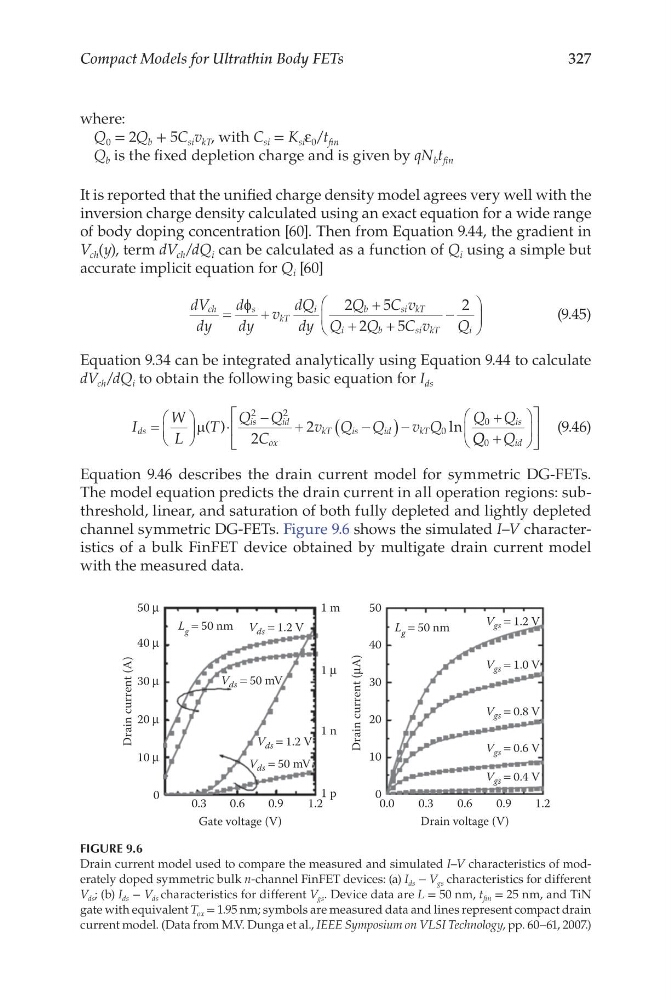
channel symmetric DG-FETs. Figure 9.6 shows the simulated I–V characteristics of a bulk FinFET device obtained by multigate drain current model
with the measured data.
0
10 μ
20 μ
30 μ
40 μ
50 μ
L g = 50 nm V ds = 1.2 V
1 m
1 μ
1 n
1 p
0.3
Gate voltage (V)
0.6
0.9
1.2
V ds = 50 mV
V ds = 1.2 V
V ds = 50 mV
Drain current (A)
V gs = 1.2 V
V gs = 1.0 V
V gs = 0.8 V
V gs = 0.6 V
V gs = 0.4 V
0.0
0
10
20
30
40
50
0.3
0.6
0.9
1.2
L g = 50 nm
Drain current (μA)
Drain voltage (V)
FIGURE 9.6
Drain current model used to compare the measured and simulated I–V characteristics of moderately doped symmetric bulk n-channel FinFET devices: (a) I ds − V gs characteristics for different
V ds ; (b) I ds − V ds characteristics for different V gs . Device data are L = 50 nm, t fin = 25 nm, and TiN
gate with equivalent T ox = 1.95 nm; symbols are measured data and lines represent compact drain
current model. (Data from M.V. Dunga et al., IEEE Symposium on VLSI Technology, pp. 60–61, 2007.)
Compact Models for Ultrathin Body FETs
where:
Q 0 = 2Q b + 5C si v kT , with C si = K si ε 0 /t fin
Q b is the fixed depletion charge and is given by qN b t fin
It is reported that the unified charge density model agrees very well with the
inversion charge density calculated using an exact equation for a wide range
of body doping concentration [60]. Then from Equation 9.44, the gradient in
V ch (y), term dV ch /dQ i can be calculated as a function of Q i using a simple but
accurate implicit equation for Q i [60]
dV
dy
d
dy
v
dQ
dy
Q
C v
Q
Q
C v
Q
ch
s
kT
i
b
si kT
i
b
si kT
i
=
+
+
+
+
−
φ
2
5
2
5
2
(9.45)
Equation 9.34 can be integrated analytically using Equation 9.44 to calculate
dV ch /dQ i to obtain the following basic equation for I ds
I
W
L
T
Q Q
C
v Q Q
v Q
Q Q
ds
is
id
ox
kT
is
id
kT
is
=
⋅
−
+
−
(
)−
+
µ( )
ln
2
2
0
0
2
2
Q Q Q id
0 +
(9.46)
Equation 9.46 describes the drain current model for symmetric DG-FETs.
The model equation predicts the drain current in all operation regions: subthreshold, linear, and saturation of both fully depleted and lightly depleted
channel symmetric DG-FETs. Figure 9.6 shows the simulated I–V characteristics of a bulk FinFET device obtained by multigate drain current model
with the measured data.
0
10 μ
20 μ
30 μ
40 μ
50 μ
L g = 50 nm V ds = 1.2 V
1 m
1 μ
1 n
1 p
0.3
Gate voltage (V)
0.6
0.9
1.2
V ds = 50 mV
V ds = 1.2 V
V ds = 50 mV
Drain current (A)
V gs = 1.2 V
V gs = 1.0 V
V gs = 0.8 V
V gs = 0.6 V
V gs = 0.4 V
0.0
0
10
20
30
40
50
0.3
0.6
0.9
1.2
L g = 50 nm
Drain current (μA)
Drain voltage (V)
FIGURE 9.6
Drain current model used to compare the measured and simulated I–V characteristics of moderately doped symmetric bulk n-channel FinFET devices: (a) I ds − V gs characteristics for different
V ds ; (b) I ds − V ds characteristics for different V gs . Device data are L = 50 nm, t fin = 25 nm, and TiN
gate with equivalent T ox = 1.95 nm; symbols are measured data and lines represent compact drain
current model. (Data from M.V. Dunga et al., IEEE Symposium on VLSI Technology, pp. 60–61, 2007.)