

326
Compact Models for Integrated Circuit Design
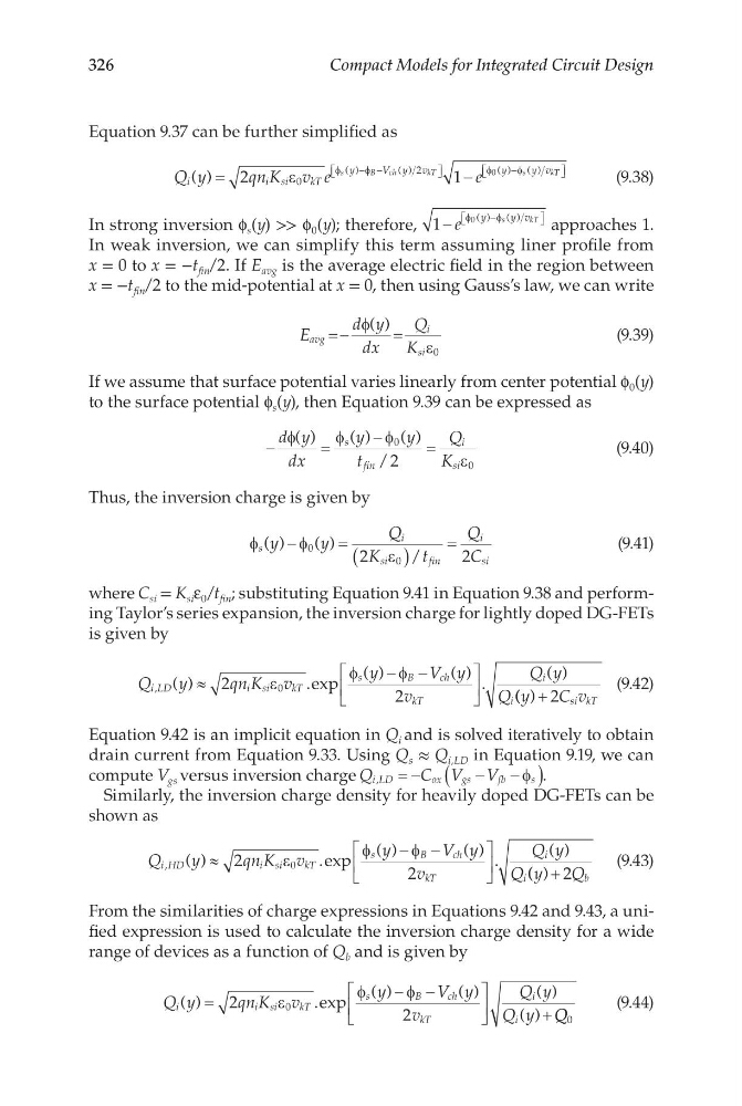
Equation 9.37 can be further simplified as
Q y
qn K v e
e
i
isi
kT
y
V y v
y
y v
s
B
ch
kT
s
k
( )
( )
( )
( )
( )
=
−
− −
−
2
1
0
2
0
ε
φ
φ
φ
φ
T T
(9.38)
In strong inversion f s (y) >> f 0 (y); therefore, 1
0
−
−
e
y
y v
s
k T
φ
φ
( )
( )
approaches 1.
In weak inversion, we can simplify this term assuming liner profile from
x = 0 to x = −t fin / 2. If E avg is the average electric field in the region between
x = −t fin / 2 to the mid-potential at x = 0, then using Gauss’s law, we can write
E
d y
dx
Q
K
avg
i
si
( )
= −
=
φ
ε 0
(9.39)
If we assume that surface potential varies linearly from center potential f 0 (y)
to the surface potential f s (y), then Equation 9.39 can be expressed as
−
=
−
=
d y
dx
y
y
t
Q
K
s
fin
i
si
φ
φ
φ
ε
( )
( )
( )
/
0
0
2
(9.40)
Thus, the inversion charge is given by
φ
φ
ε
s
i
si
fin
i
si
y
y
Q
K
t
Q
C
( )
( )
/
−
= (
)
=
0
0
2
2
(9.41)
where C si = K si ε 0 /t fin ; substituting Equation 9.41 in Equation 9.38 and performing Taylor’s series expansion, the inversion charge for lightly doped DG-FETs
is given by
Q
y
qn K v
y
V y
v
Q y
Q
i LD
isi
kT
s
B
ch
kT
i
i
, ( )
.exp
( )
( ) .
( )
≈
− −
2
2
0
ε
φ
φ
( ( )
y
C v
si kT
+ 2
(9.42)
Equation 9.42 is an implicit equation in Q i and is solved iteratively to obtain
drain current from Equation 9.33. Using Q s ≈ Q i,LD in Equation 9.19, we can
compute V gs versus inversion charge Q
C V V
i LD
o x
g s
f b
s
,
= −
−
−
(
)
φ .
Similarly, the inversion charge density for heavily doped DG-FETs can be
shown as
Q
y
qn K v
y
V y
v
Q y
Q
i HD
isi
kT
s
B
ch
kT
i
i
,
( )
.exp
( )
( ) .
( )
≈
− −
2
2
0
ε
φ
φ
( ( )
y
Q b
+ 2
(9.43)
From the similarities of charge expressions in Equations 9.42 and 9.43, a unified expression is used to calculate the inversion charge density for a wide
range of devices as a function of Q b and is given by
Q y
qn K v
y
V y
v
Q y
Q y
i
isi
kT
s
B
ch
kT
i
i
( )
.exp
( )
( )
( )
( )
=
− −
+
2
2
0
ε
φ
φ
Q Q 0
(9.44)
Compact Models for Integrated Circuit Design
Equation 9.37 can be further simplified as
Q y
qn K v e
e
i
isi
kT
y
V y v
y
y v
s
B
ch
kT
s
k
( )
( )
( )
( )
( )
=
−
− −
−
2
1
0
2
0
ε
φ
φ
φ
φ
T T
(9.38)
In strong inversion f s (y) >> f 0 (y); therefore, 1
0
−
−
e
y
y v
s
k T
φ
φ
( )
( )
approaches 1.
In weak inversion, we can simplify this term assuming liner profile from
x = 0 to x = −t fin / 2. If E avg is the average electric field in the region between
x = −t fin / 2 to the mid-potential at x = 0, then using Gauss’s law, we can write
E
d y
dx
Q
K
avg
i
si
( )
= −
=
φ
ε 0
(9.39)
If we assume that surface potential varies linearly from center potential f 0 (y)
to the surface potential f s (y), then Equation 9.39 can be expressed as
−
=
−
=
d y
dx
y
y
t
Q
K
s
fin
i
si
φ
φ
φ
ε
( )
( )
( )
/
0
0
2
(9.40)
Thus, the inversion charge is given by
φ
φ
ε
s
i
si
fin
i
si
y
y
Q
K
t
Q
C
( )
( )
/
−
= (
)
=
0
0
2
2
(9.41)
where C si = K si ε 0 /t fin ; substituting Equation 9.41 in Equation 9.38 and performing Taylor’s series expansion, the inversion charge for lightly doped DG-FETs
is given by
Q
y
qn K v
y
V y
v
Q y
Q
i LD
isi
kT
s
B
ch
kT
i
i
, ( )
.exp
( )
( ) .
( )
≈
− −
2
2
0
ε
φ
φ
( ( )
y
C v
si kT
+ 2
(9.42)
Equation 9.42 is an implicit equation in Q i and is solved iteratively to obtain
drain current from Equation 9.33. Using Q s ≈ Q i,LD in Equation 9.19, we can
compute V gs versus inversion charge Q
C V V
i LD
o x
g s
f b
s
,
= −
−
−
(
)
φ .
Similarly, the inversion charge density for heavily doped DG-FETs can be
shown as
Q
y
qn K v
y
V y
v
Q y
Q
i HD
isi
kT
s
B
ch
kT
i
i
,
( )
.exp
( )
( ) .
( )
≈
− −
2
2
0
ε
φ
φ
( ( )
y
Q b
+ 2
(9.43)
From the similarities of charge expressions in Equations 9.42 and 9.43, a unified expression is used to calculate the inversion charge density for a wide
range of devices as a function of Q b and is given by
Q y
qn K v
y
V y
v
Q y
Q y
i
isi
kT
s
B
ch
kT
i
i
( )
.exp
( )
( )
( )
( )
=
− −
+
2
2
0
ε
φ
φ
Q Q 0
(9.44)