

318
Compact Models for Integrated Circuit Design
In a UTB transistor, the thickness of the buried oxide (BOx) layer is reduced
to use the substrate immediately below the BOx as a back gate to bias the
body of the device and to enable a multi-V th technology, especially for systemon-chip design [54–56].
The multiple-gate FET structures can be classified as (1) common multigate (CMG) structure where a common gate terminal is used to bias the
device and the gate dielectric thicknesses is the same and (2) independent
multigate (IMG) structure where gates are independently biased and the
gate dielectric thickness is different for each gate.
9.3 Common Multiple-Gate FinFET Model
The term common gate defines all gates in the multigate (double-gate or
triple-gate or quadruple-gate) FinFET, which are electrically interconnected
and are biased at the same electrical terminal voltage. It is also assumed
that the gate work functions and the dielectric thicknesses on all sides to the
silicon fin are the same. However, the carrier mobilities in the inversion are
dependent on crystal orientations and/or strain.
9.3.1 Core Model: Poisson-Carrier Transport
The core CMG model is formulated using gradual channel approximation
(GCA) [57], described in Chapter 4, and assuming physical effects such as
mobility degradation can safely be neglected. Several basic models have
been proposed for the FinFET, where charge [58] and surface potential [59,60]
modeling approaches have been mainly used for model formulations. The
core model described in the following section is based on the solution of
Poisson’s drift/diffusion equations for a long channel DG-FinFET assuming
a finite doping in the channel [29]. The reported simulation data obtained
by the core model agree very well with the numerical device simulation
data [60,61].
9.3.1.1 Electrostatics
For the simplicity of model formulation, let us consider 2D (two-dimensional)
cross section of an ideal n-type FinFET device structure as a common doublegate transistor as shown in Figure 9.5. First of all, we obtain surface potential
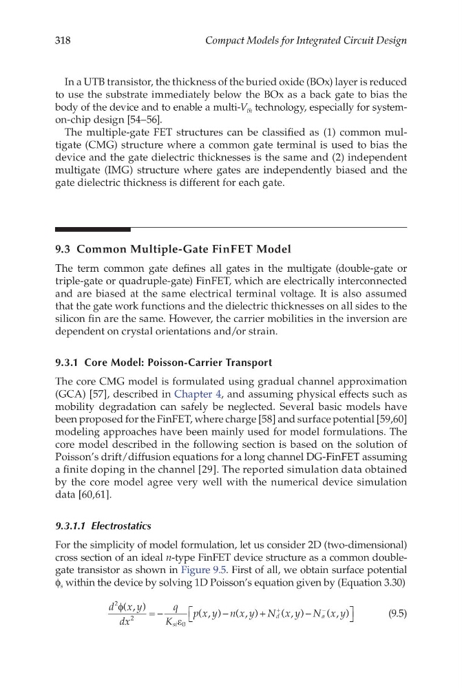
f s within the device by solving 1D Poisson’s equation given by (Equation 3.30)
d x y
dx
q
K
p x y n x y N x y N x y
si
d
a
2
2
0
φ
ε
( , )
( , ) ( , )
( , )
( , )
= −
−
+
−
+
−
(9.5)
Compact Models for Integrated Circuit Design
In a UTB transistor, the thickness of the buried oxide (BOx) layer is reduced
to use the substrate immediately below the BOx as a back gate to bias the
body of the device and to enable a multi-V th technology, especially for systemon-chip design [54–56].
The multiple-gate FET structures can be classified as (1) common multigate (CMG) structure where a common gate terminal is used to bias the
device and the gate dielectric thicknesses is the same and (2) independent
multigate (IMG) structure where gates are independently biased and the
gate dielectric thickness is different for each gate.
9.3 Common Multiple-Gate FinFET Model
The term common gate defines all gates in the multigate (double-gate or
triple-gate or quadruple-gate) FinFET, which are electrically interconnected
and are biased at the same electrical terminal voltage. It is also assumed
that the gate work functions and the dielectric thicknesses on all sides to the
silicon fin are the same. However, the carrier mobilities in the inversion are
dependent on crystal orientations and/or strain.
9.3.1 Core Model: Poisson-Carrier Transport
The core CMG model is formulated using gradual channel approximation
(GCA) [57], described in Chapter 4, and assuming physical effects such as
mobility degradation can safely be neglected. Several basic models have
been proposed for the FinFET, where charge [58] and surface potential [59,60]
modeling approaches have been mainly used for model formulations. The
core model described in the following section is based on the solution of
Poisson’s drift/diffusion equations for a long channel DG-FinFET assuming
a finite doping in the channel [29]. The reported simulation data obtained
by the core model agree very well with the numerical device simulation
data [60,61].
9.3.1.1 Electrostatics
For the simplicity of model formulation, let us consider 2D (two-dimensional)
cross section of an ideal n-type FinFET device structure as a common doublegate transistor as shown in Figure 9.5. First of all, we obtain surface potential
f s within the device by solving 1D Poisson’s equation given by (Equation 3.30)
d x y
dx
q
K
p x y n x y N x y N x y
si
d
a
2
2
0
φ
ε
( , )
( , ) ( , )
( , )
( , )
= −
−
+
−
+
−
(9.5)